
Neon VUEQ
Contents
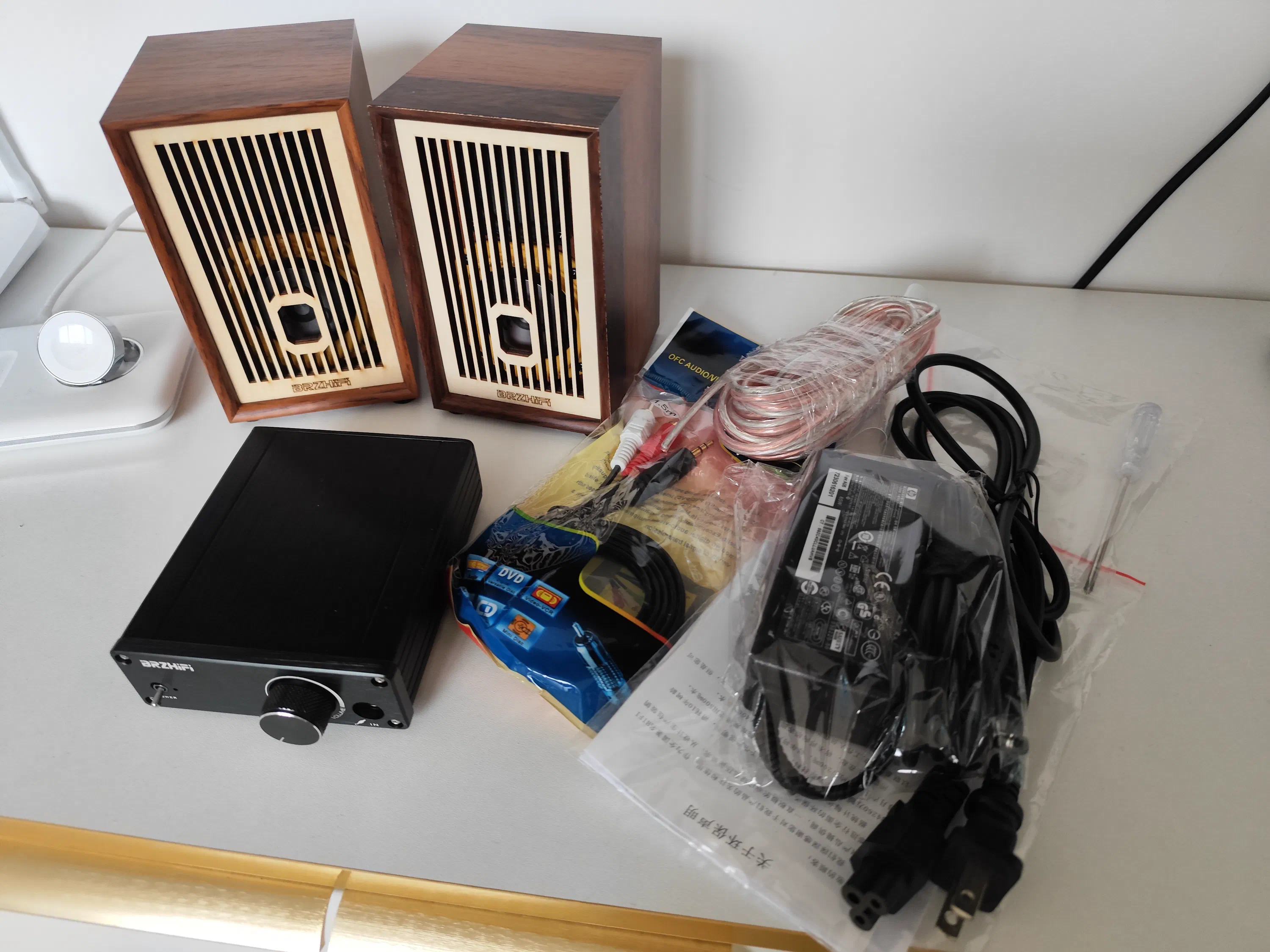
This project emerged after I bought my BRZ HiFi mini bookshelf speakers. Even after modding the amp with better coupling capacitors, the bass response still wasn’t very satisfactory and felt like it didn’t bring the full potential out of these adorable speakers. So I got to work designing an op-amp based EQ to remediate this, I didn’t want something massively complex like a full parametric EQ and just settled on a high and low shelf as being enough.
Using my uncalibrated condenser microphone and RoomEQWizard, I made a rough attempt to record the output spectrum raw from the speakers using the BRZHiFi amp they came with (after I modded that too):
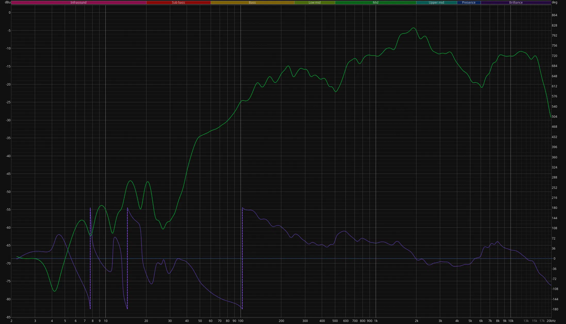
As we can see, while it is relatively flat from 200Hz to 16kHz, the low end leaves a lot to be desired; as is to be expected with physically small speakers. Definitely big room for improvement with active EQ.
But then it struck me that this would be a great opportunity to build a satisfying VU meter that I’ve been wanting to do for a long time. Unable to easily get my hands on analog needle style meters, I decided to create a digital meter using neon lamps for their mesmerising glow.
Design
One of the key design targets was that the final build shouldn’t be just a gimmick; I wanted both the EQ and VU meter to be calibrated and precise as a tool, rather than just pretty visuals in a black box. This heavily influenced the approach for the front-panel UI design as well as increasing the complexity of the VU meter to meet some standards.
Analog Shelf Circuits
I started by looking for active low and high shelf op-amp circuits, when I came across this great article by Douglas Self on audioxpress. The circuits from this article appealed to me as they were very well designed and some optimisation work was done. Most crucially the shown high and low shelves had well defined EQ behaviours with a gain set in dB and variable frequency ranges.
Starting with the high shelf:
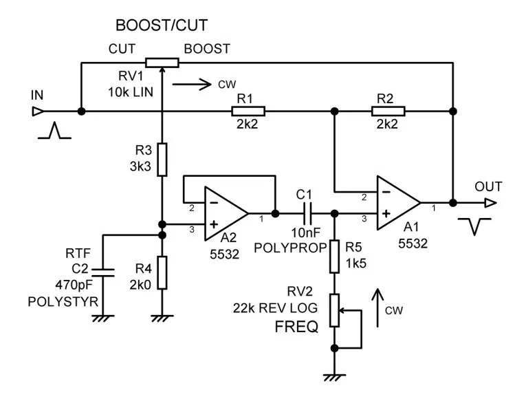
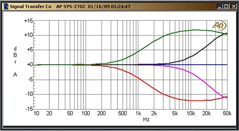
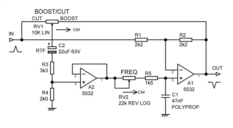
With the circuit above, we can create a high shelf with variable gain from -12dB to +12dB, and -1dB frequency from 2kHz to 20kHz. Benefiting from the noise improvements and the return-to-flat (RTF) capacitor from Douglas’s design. This ensures that there is unity gain outside the audio band and distortion stays low, theoretically reaching a 0.0004% THD. Although I substituted the 5532 op-amps for TL072/4’s for cost reasons, which should increase this figure a bit. Now for the low shelf:
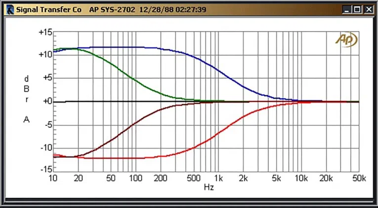
Here we have a similar story, with the same variable gain range and a -1dB frequency from 40-600Hz. Noting that the RTF capacitor needed in this case is 22uF which slightly increases the size of the circuit. In my design I also made some modifications in order to have this circuit operate from a ±2.5V split-rail setup, using another op-amp as a current buffer for that mid-rail virtual ground. The final resulting schematic for both shelves in my design is shown below:
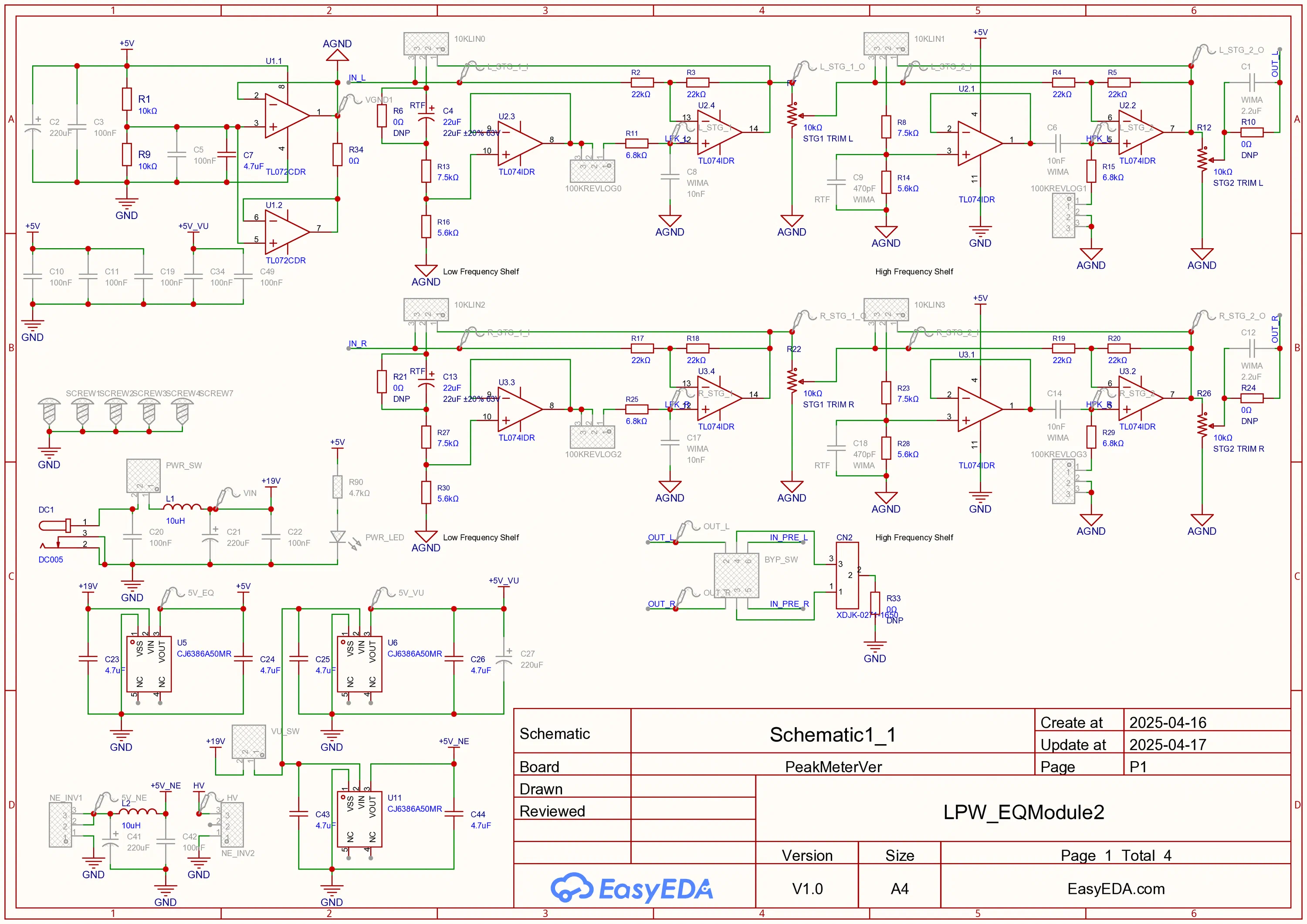
Some SMD trimmer potentiometers were added in the case that I would need to attenuate some of the audio signals coming from the output of each stage in case they clipped with my limited 5Vpk-pk headroom, but in the end this was not needed as the consumer line inputs usually didn’t exceed -5dBu or 1.232V peak at which a 12dB boost would cause clipping. They can be safely removed from the design.
In order to match my precision requirements, by exploiting the fact the the VU meter is digitally driven; I came up with the idea of displaying the exact selected frequencies on the front panel by having fixed frequencies printed on the panel and then having the corresponding neon lit up by the MCUs when a frequency knob is adjusted. To achieve this I would have to calibrate the analog voltage readings read by the MCU to the corresponding frequency points and then determine the steps to use for the 12 neon lights. This was done with a simple spreadsheet and allowed me to plan exactly how the calibration would be done, as well as what values to have printed on the front panel.
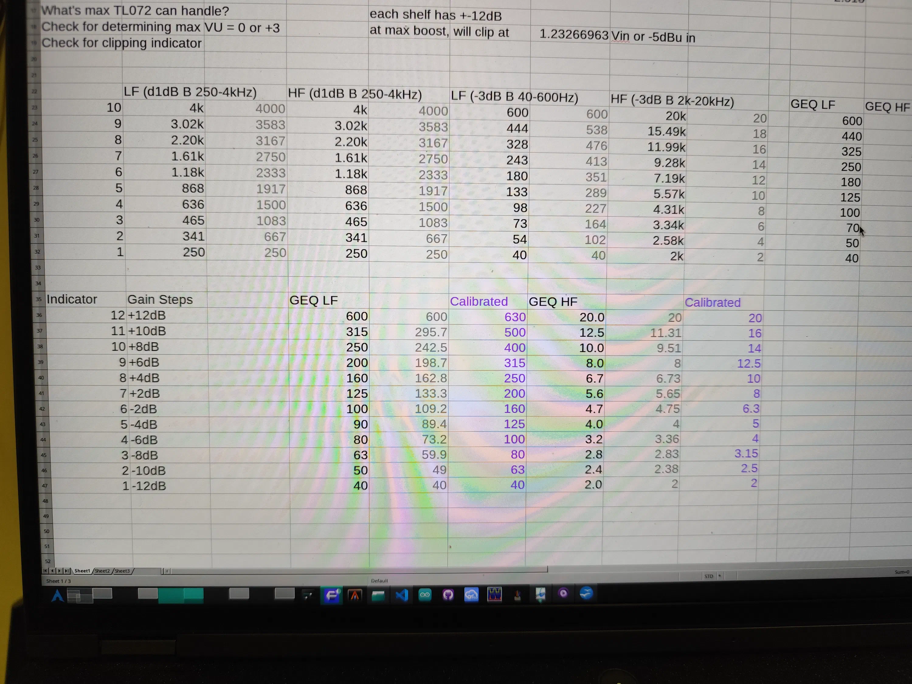
I also used this spreadsheet to do a logarithmic extrapolation to find which increments I would actually split the frequency bands into 12 steps, which was trickier than I thought as there isn’t really a standard across different brands of equalisers. I additionally pre-calculated in another sheet some of the expected MCU ADC values given the resolution and dBV voltages expected from the average and peak detectors to ease the MCU programming later.
Analog Average and Peak Detector Circuits
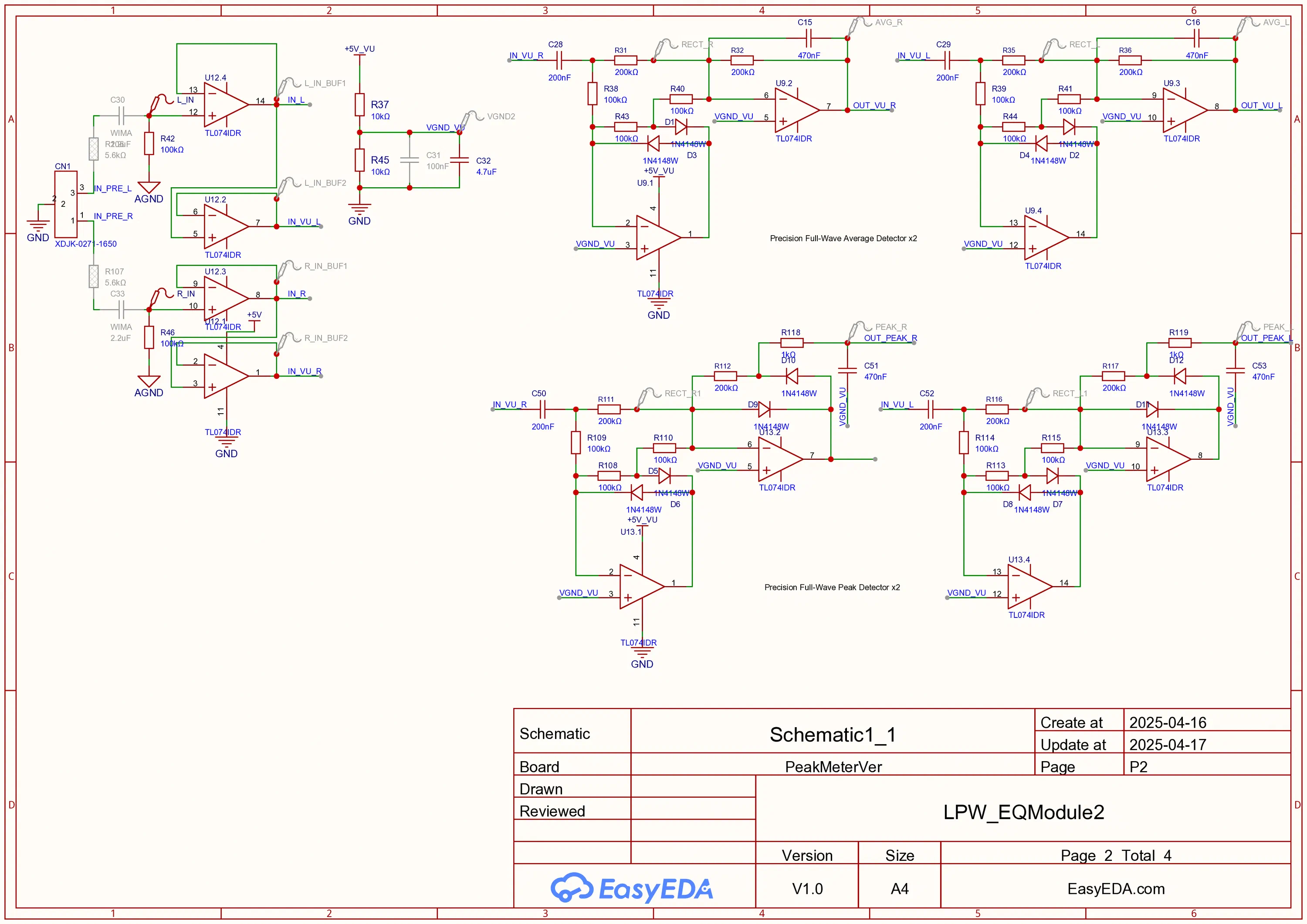
Going with the precision instrument theme, I also wanted to make sure that the VU meter was actually useful as an instrument and not just pretty to watch. This meant adhering to the ANSI C16.5-1942 standard; which specifies a range of -20dB to +3dB and a rise/fall time of 300ms for the average. Unfortunately, due to the 5V split design (which was needed to ensure compatibility with the MCU ADC input voltage range to begin with) and the fact that we are reading linear values and then mapping them to the dB logarithmic scale; meant that resolution below -20dB until -30dB wasn’t very accurate. That aside, I took great care in implementing an analog precision integrator for the average meter; using a circuit with an RC time-constant matching approximately 300ms.
To avoid the very truthful joke that VU meters are useless because they only show average loudness values and not peak values as well, which is more critical when setting up proper gain-staging with real equipment; I also decided to add a whole precision rectifier peak detector circuit to each channel. This resulted in the following schematic:
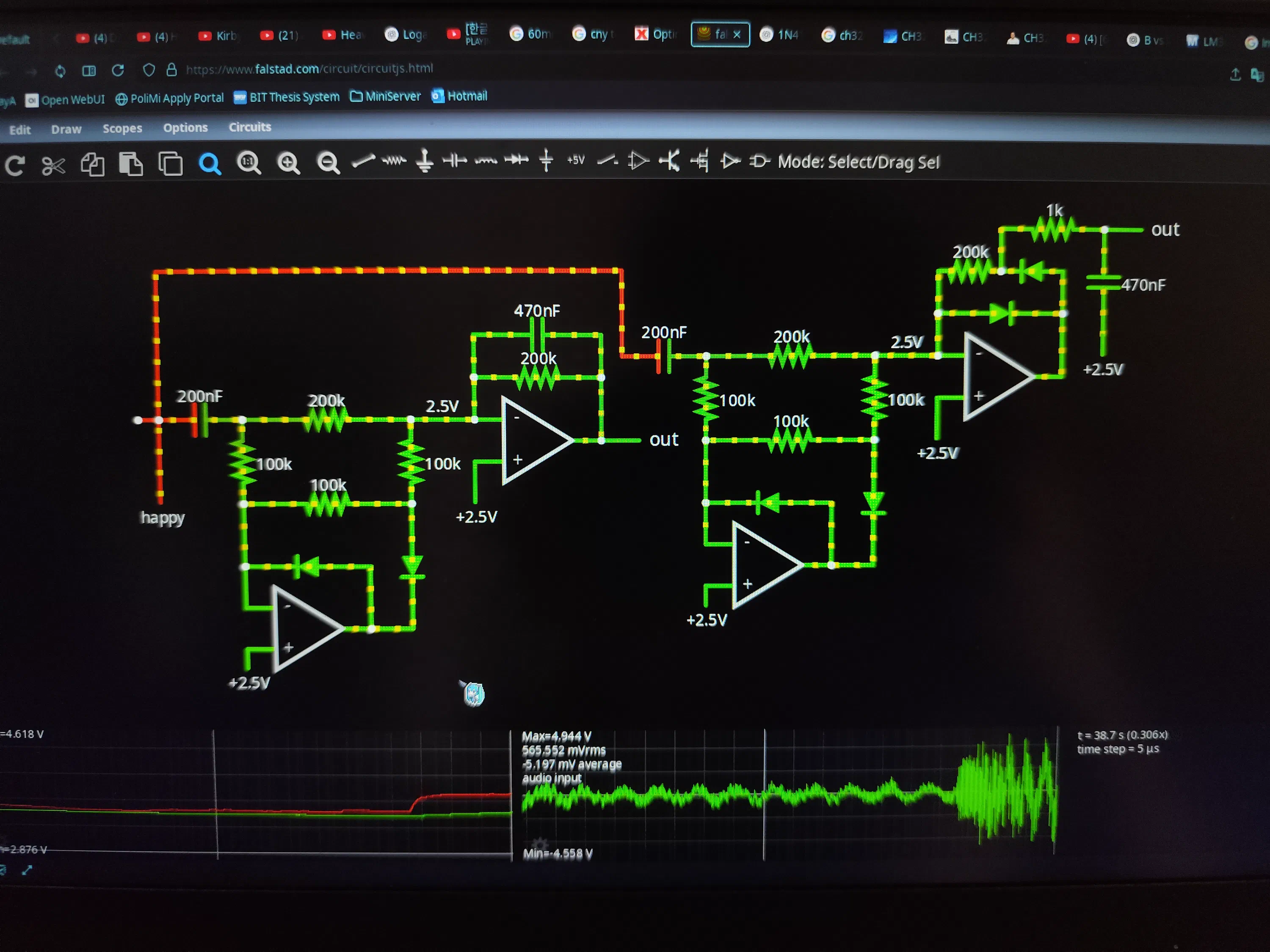
Where we can see the precision full-wave average detector on the left, and the precision full-wave peak detector on the right. I experimented and tested with different values and circuit configurations using a CircuitJS simulation.
Ideally the circuit could be further optimised so that the first precision full-wave rectifier part is reused across both detectors; but due to probably needing 2 op-amp buffers to reuse the circuit without interference, I decided it was simpler to just have the one extra op-amp and a few passives of the duplicated circuit rather than 2 additional op-amps for those two buffers. Duplicating this circuit for each channel, we get the final schematic below:
Digital VU Meter Circuit
Since we needed to switch high voltage (80-160V) to drive the neon’s anyway, and I wanted those neat UI features to show the adjusted parameters and merge the average and peak displays; I went with a digital circuit to drive the neons. The first part is a straight forward high-voltage logic-level BJT driver for the neon display. For which I picked 2N5551 BJTs, which have a 160V Collector-Emitter voltage rating at up to 600mA.
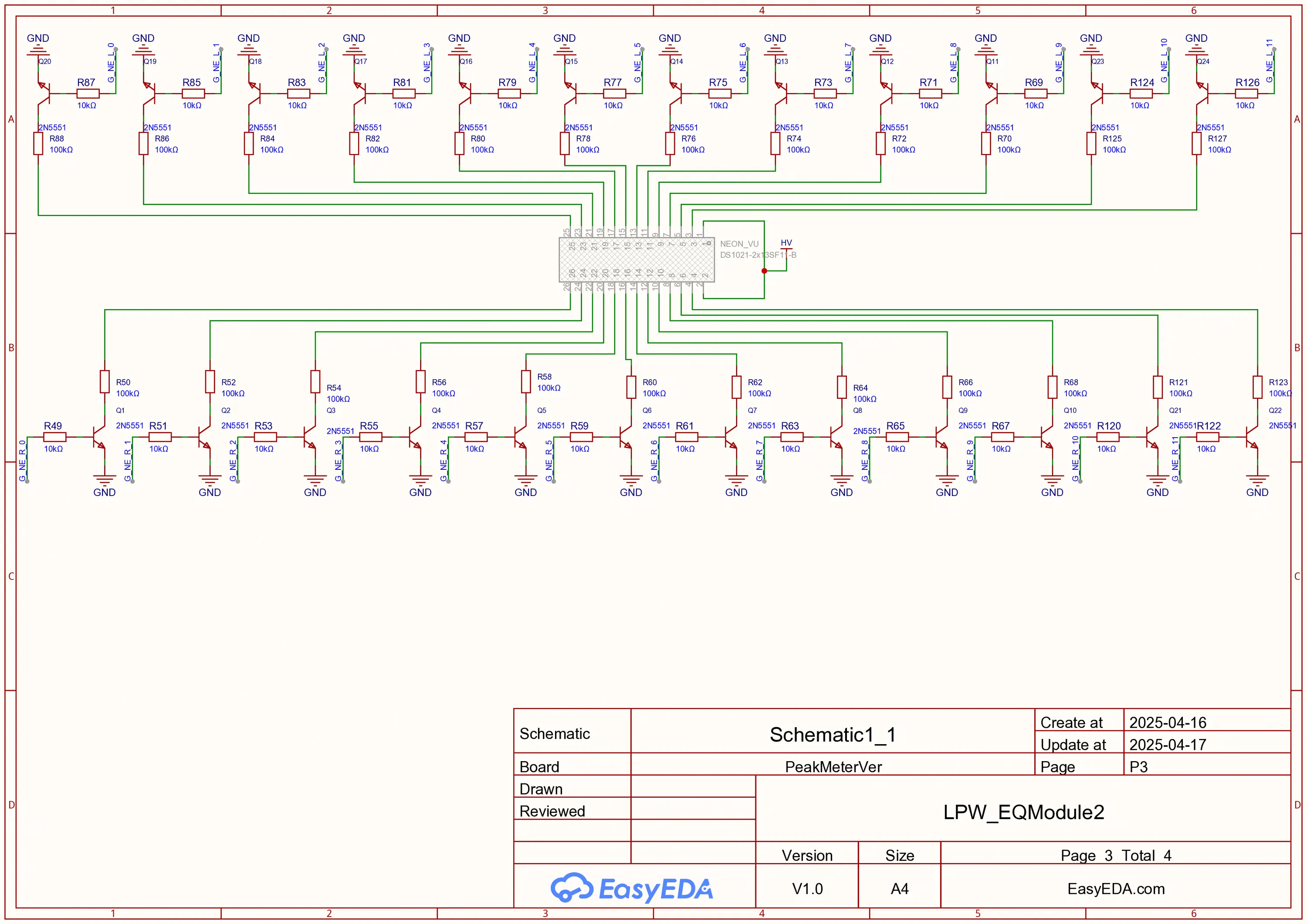
Then for the MCU, I made a peculiar choice. I knew that per audio channel I would need 4 ADC channels (peak, average, frequency knob readout, gain knob readout), as well as 12 digital outputs to drive the row of neons, and an additional digital output for a potentiometer readout enable to save current. This exact configuration was fulfilled perfectly by the TSSOP-20 version of the CH32V003 MCU, the CH32V003F4P6. I had a great deal of success using these very low-cost MCUs with CNLohr’s ch32fun open source minimal stack for these little RISC-V MCUs. This also simplified the programming a bit, as I would need 2 MCUs, one per channel. Allowing me to have the same code for both MCUs with just different calibration defines for the different frequency ranges to display.
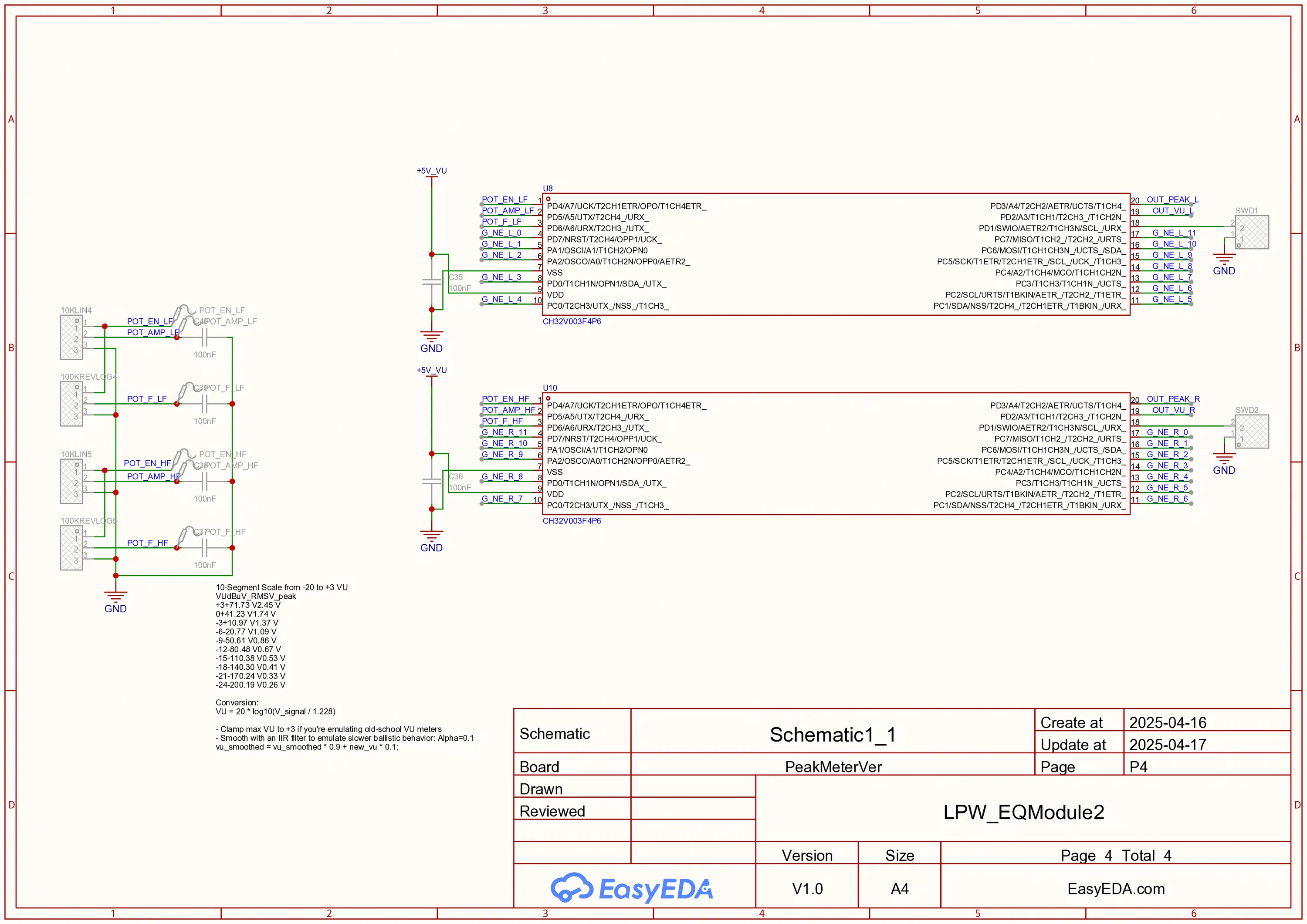
I will further detail the MCU firmware in the upcoming section about the first prototype.
PCB Design
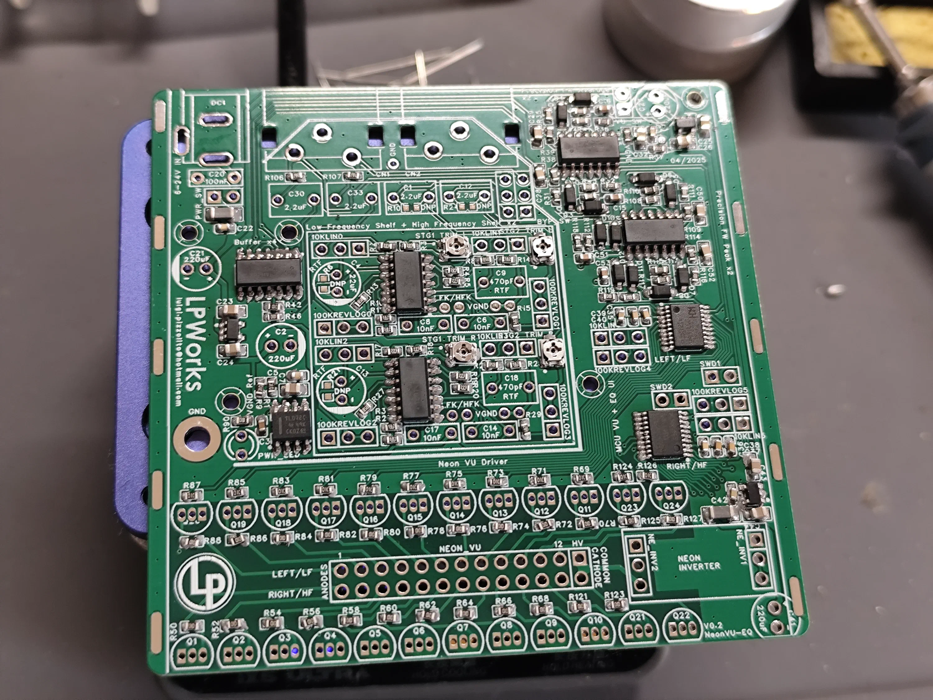
With the circuit complete, I started the PCB design by sectioning off the analog and digital sections after placing the components to organise my ground splits. I went with a four layer design to have much closer ground planes and hopefully completely eliminate the noise ground-floor from being audible from the speakers.
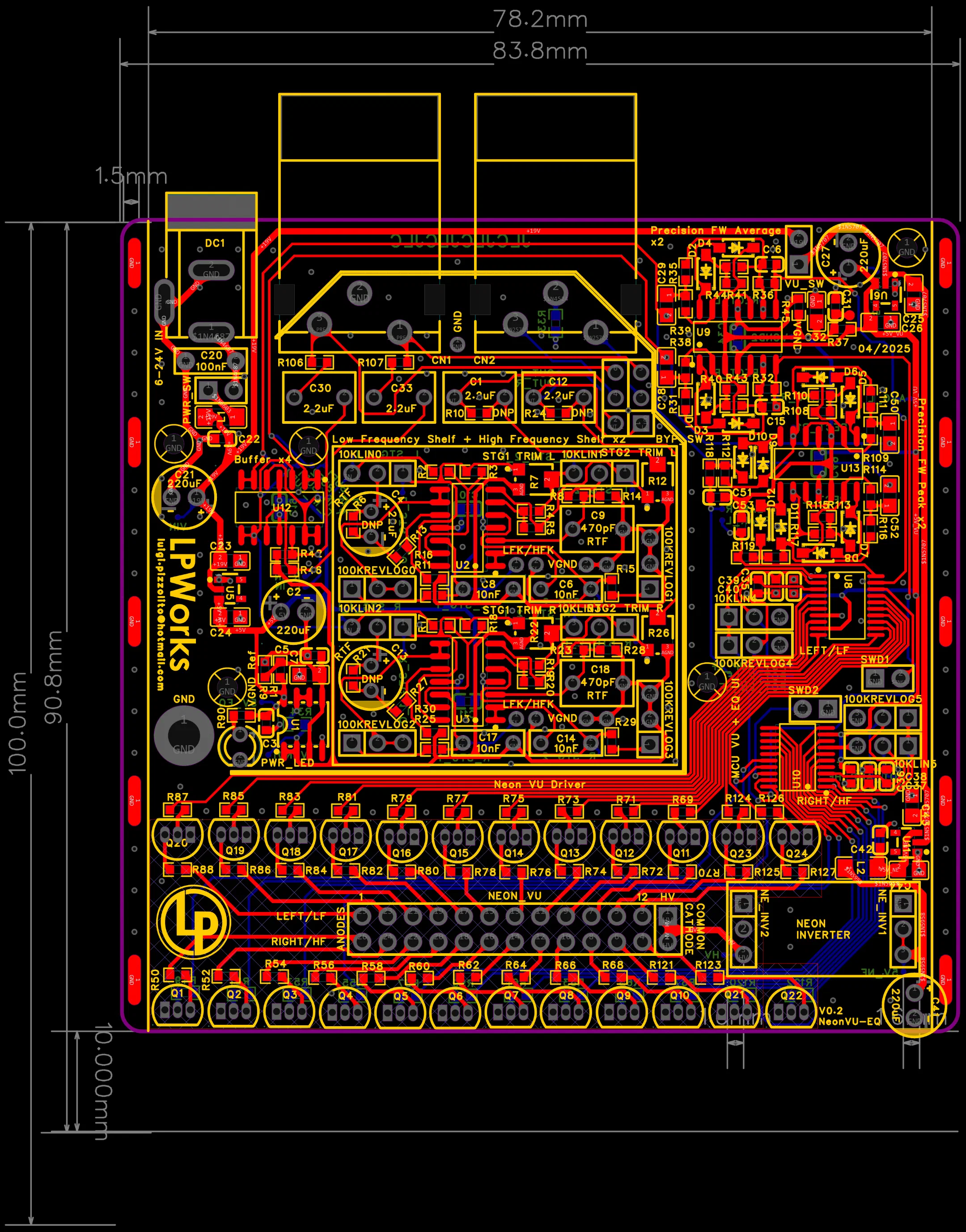
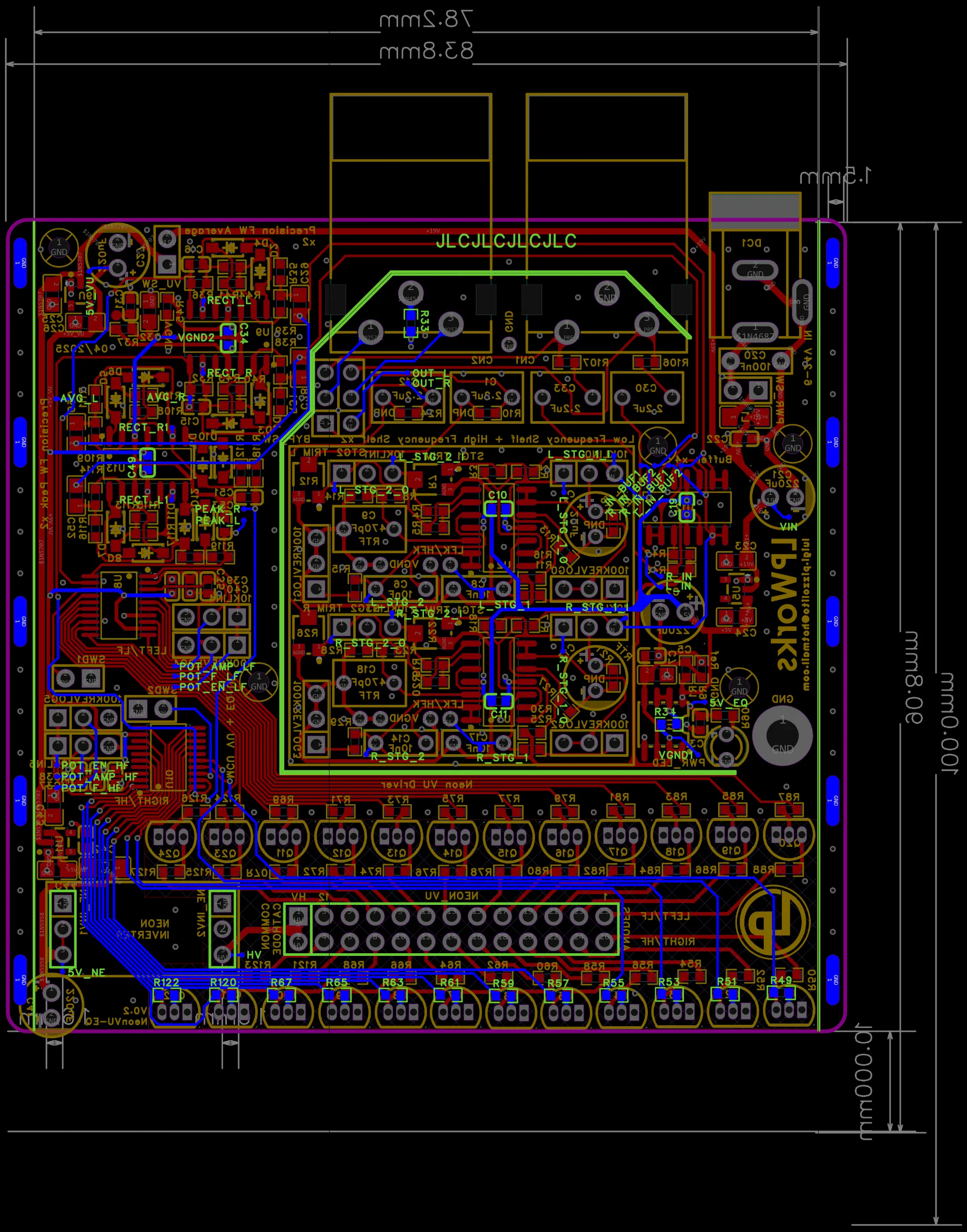
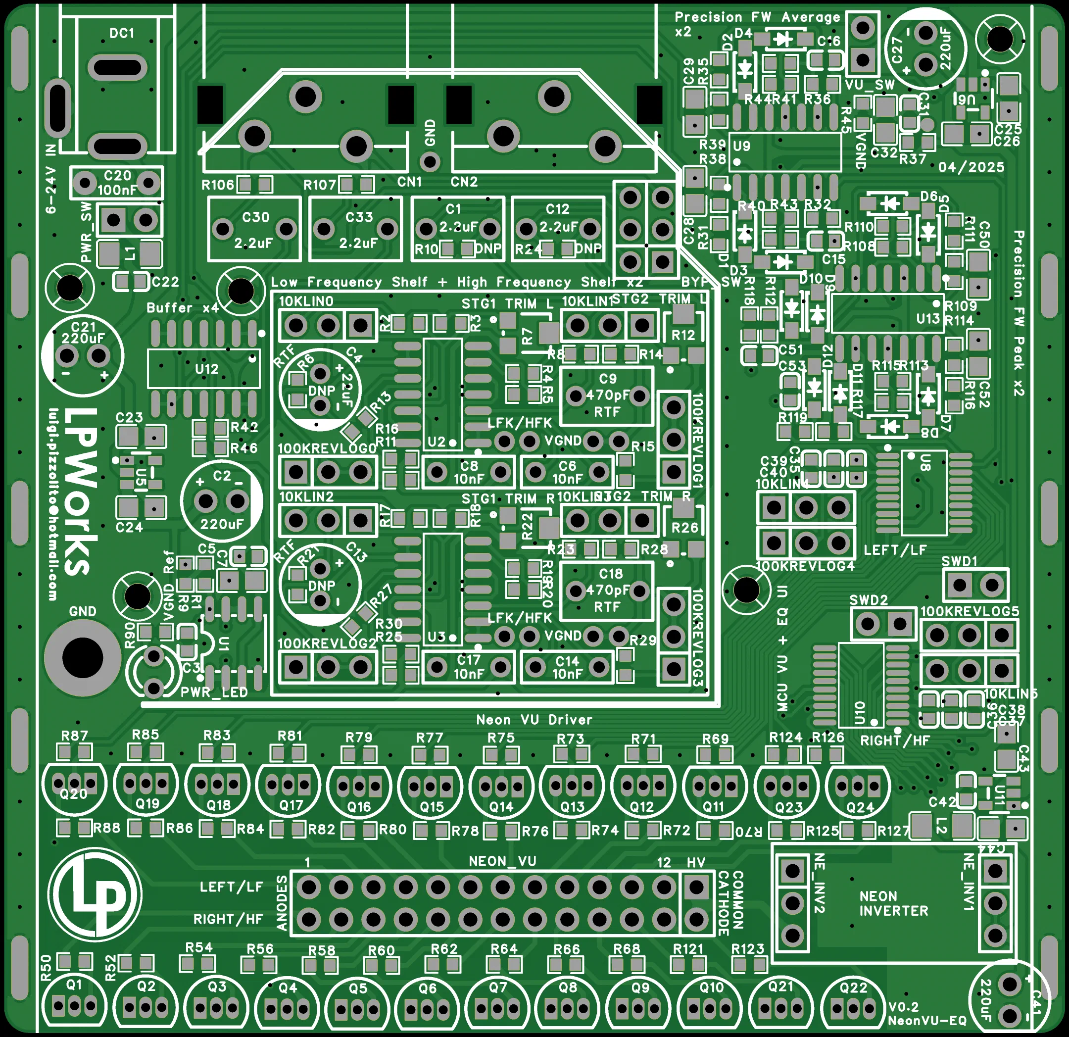
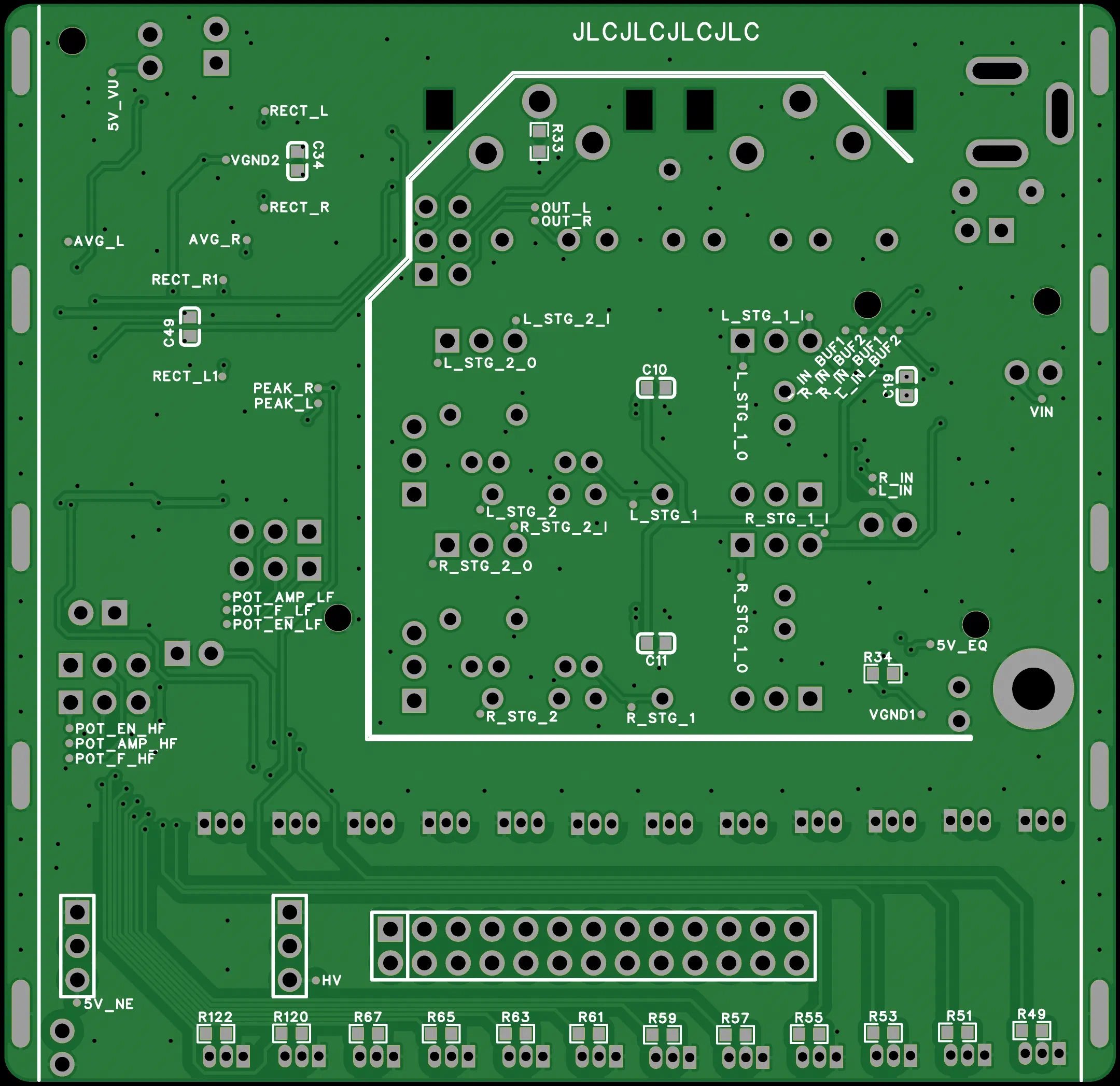
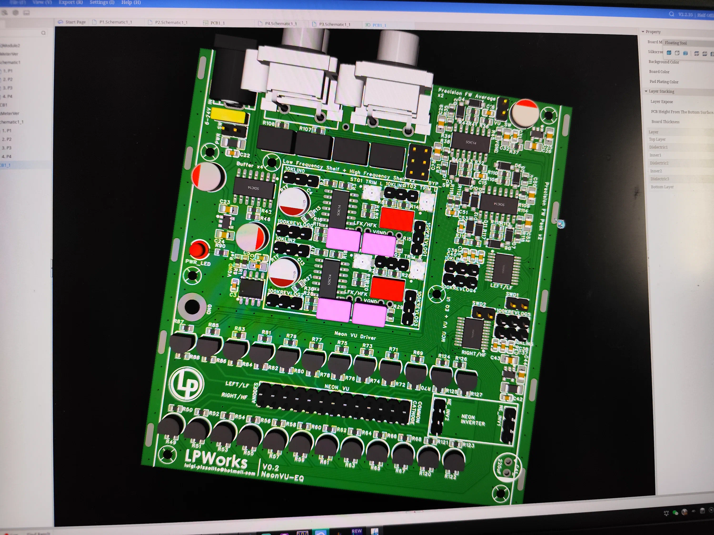
This was not easy at all to route and took many hours, even sneaking some SMD components onto the bottom side. I left space to be able to use some higher quality WIMA film capacitors and solid-state electrolytics; to avoid distortion in the audio path and to avoid long-term capacitor plague.
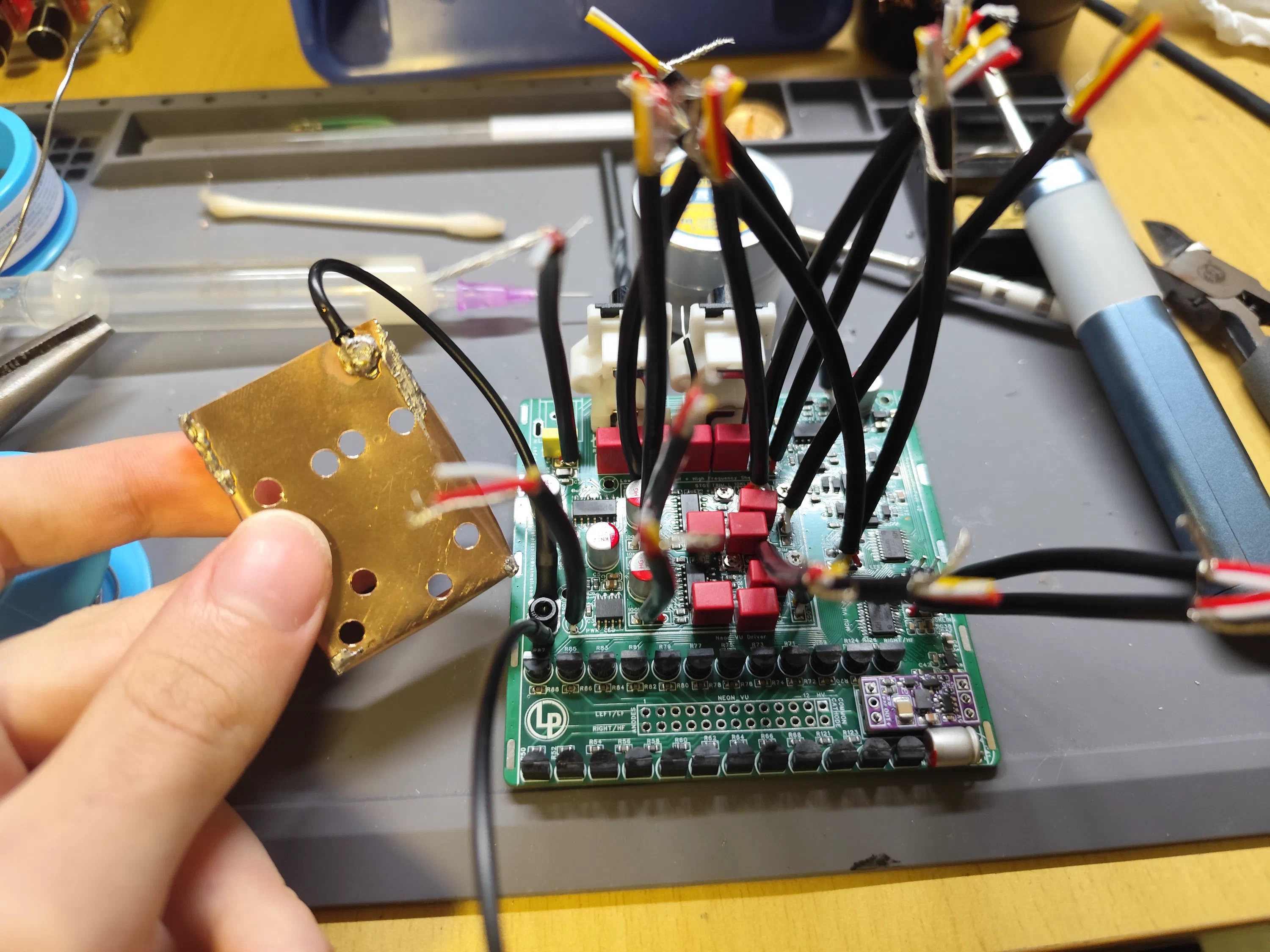
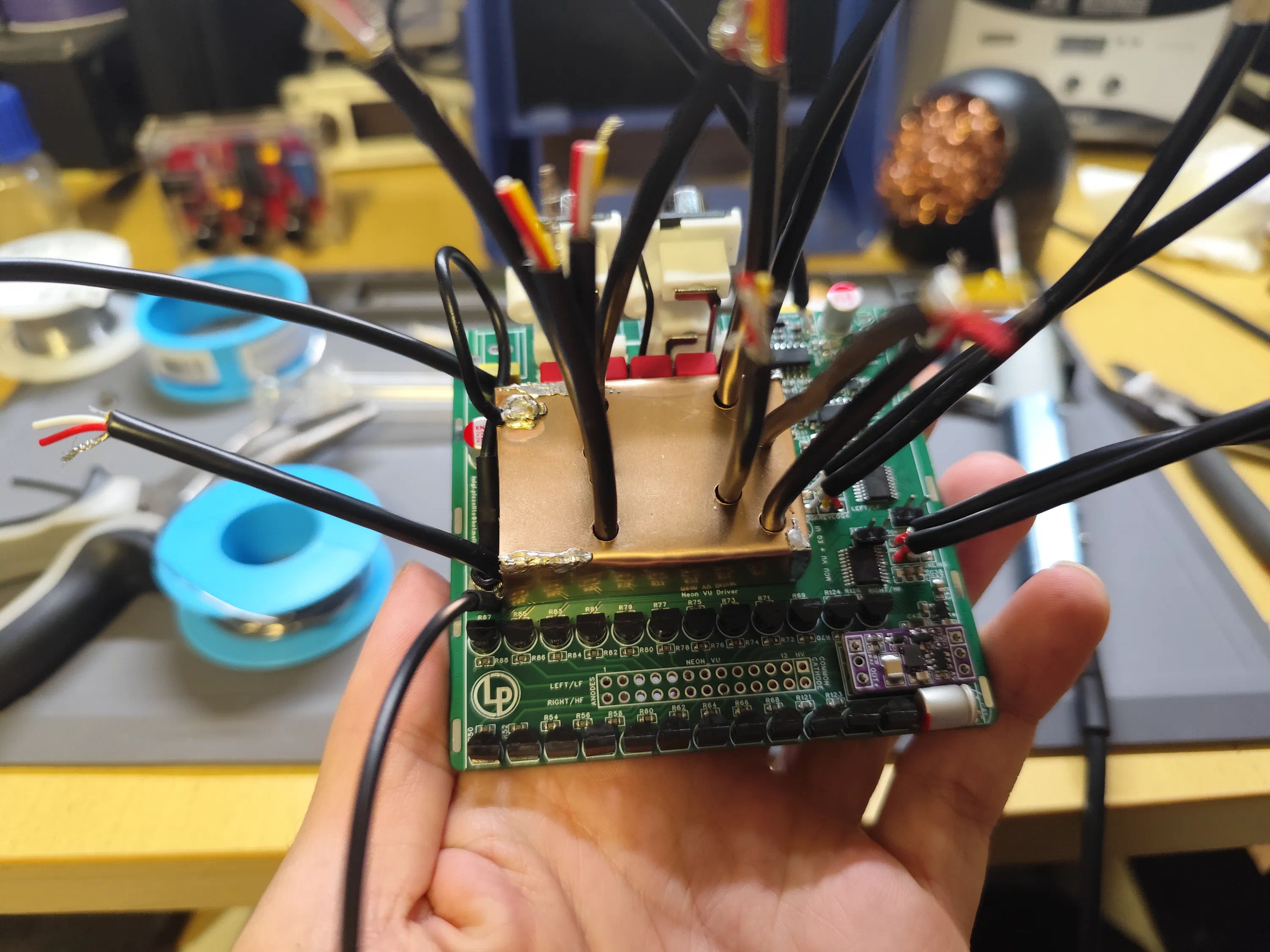
Unfortunately, the board was so tight inside of the extruded aluminium case that I had picked for it, that many of the connections had to be hand soldered by wire later. This included the connection to all of the potentiometers, as well as the 26 lines used to drive the neon display. I would later come to regret this as it greatly increased the labour and time of the build. Particularly as I designed for a copper RF shield over the analog section which required drilling to feed through the shielded 3-core cable I used for the potentiometer connections as those carried audio signals which I did not want to pickup any noise from the HV DC converter driving the neon circuit.
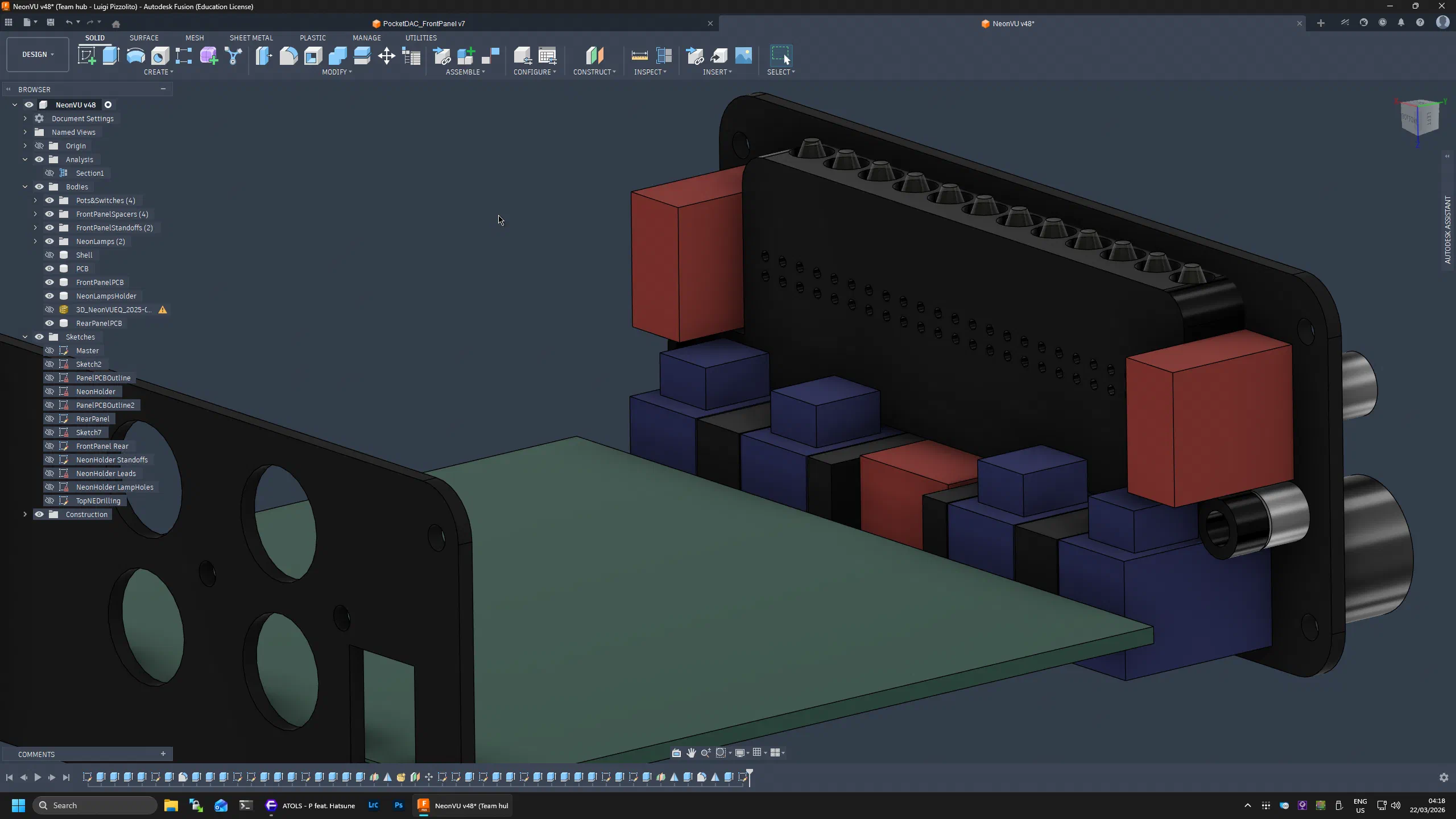
Another questionable choice was just how tight the front-panel ended up becoming, which didn’t allow me to traditionally mount the potentiometers on the main PCB and required all of the triple pots to be hand wired (that’s nine connections for each of the four pots, aka. Over 74 hand-wired connections in total).
Case and Panel Design
Then for the front and back panel design, it was a painful process of modelling everything in Fusion 360 and packing it tight with my UI while ensuring everything would fit. The initial design was done in CAD:
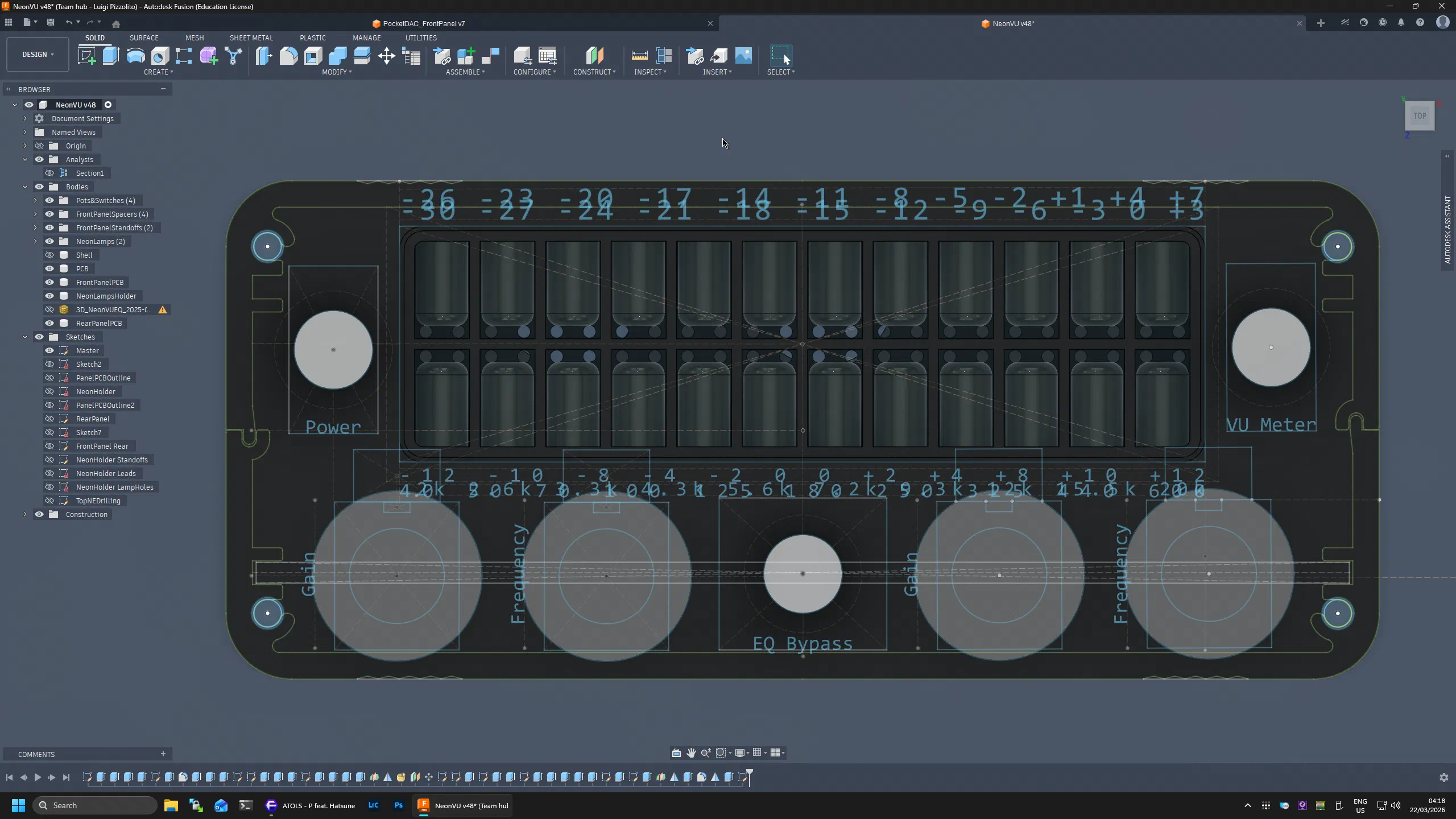
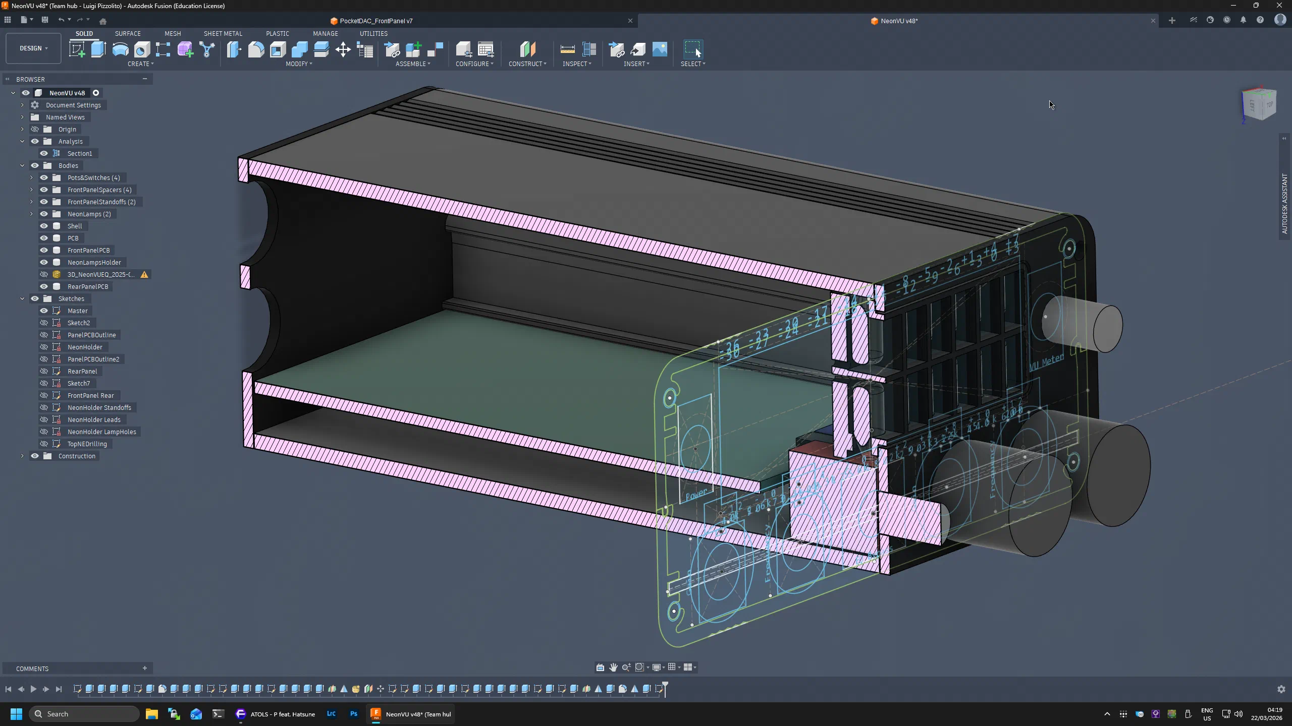
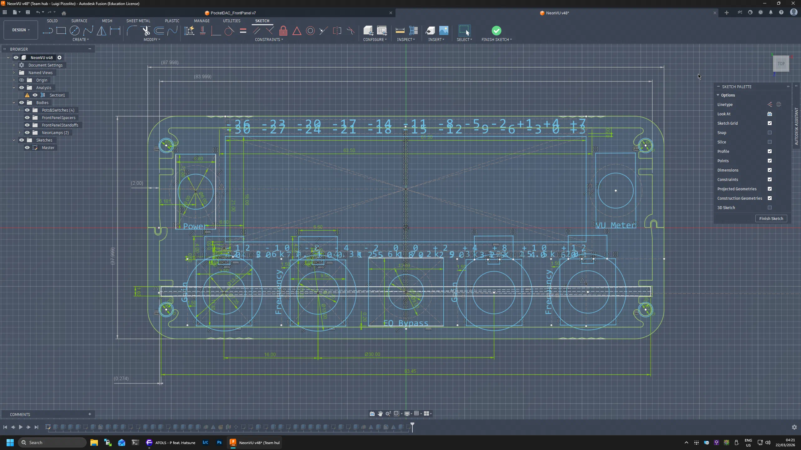
Which was then later exported as SVGs and imported into EasyEDA for the final design, as I decided to use PCBs to create the front and back panel conveniently with the correct drilling and silkscreening.
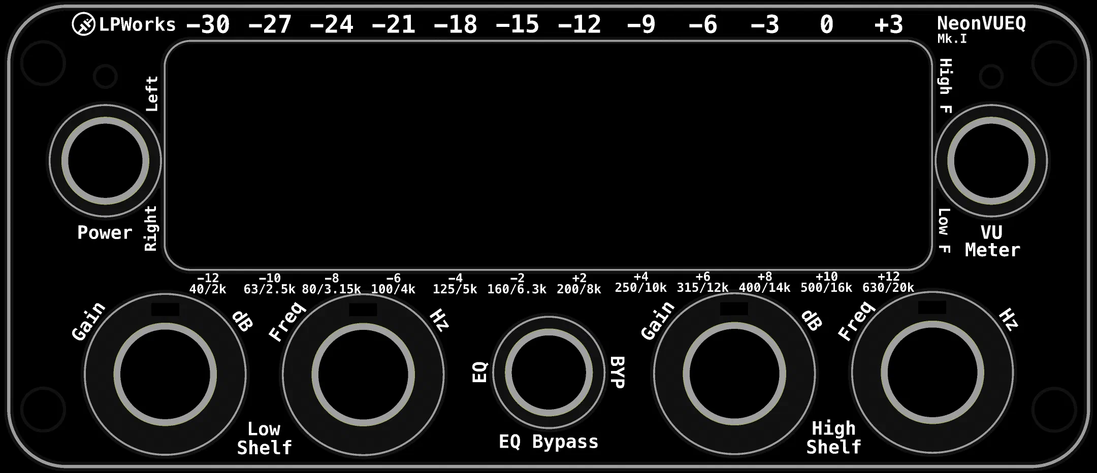
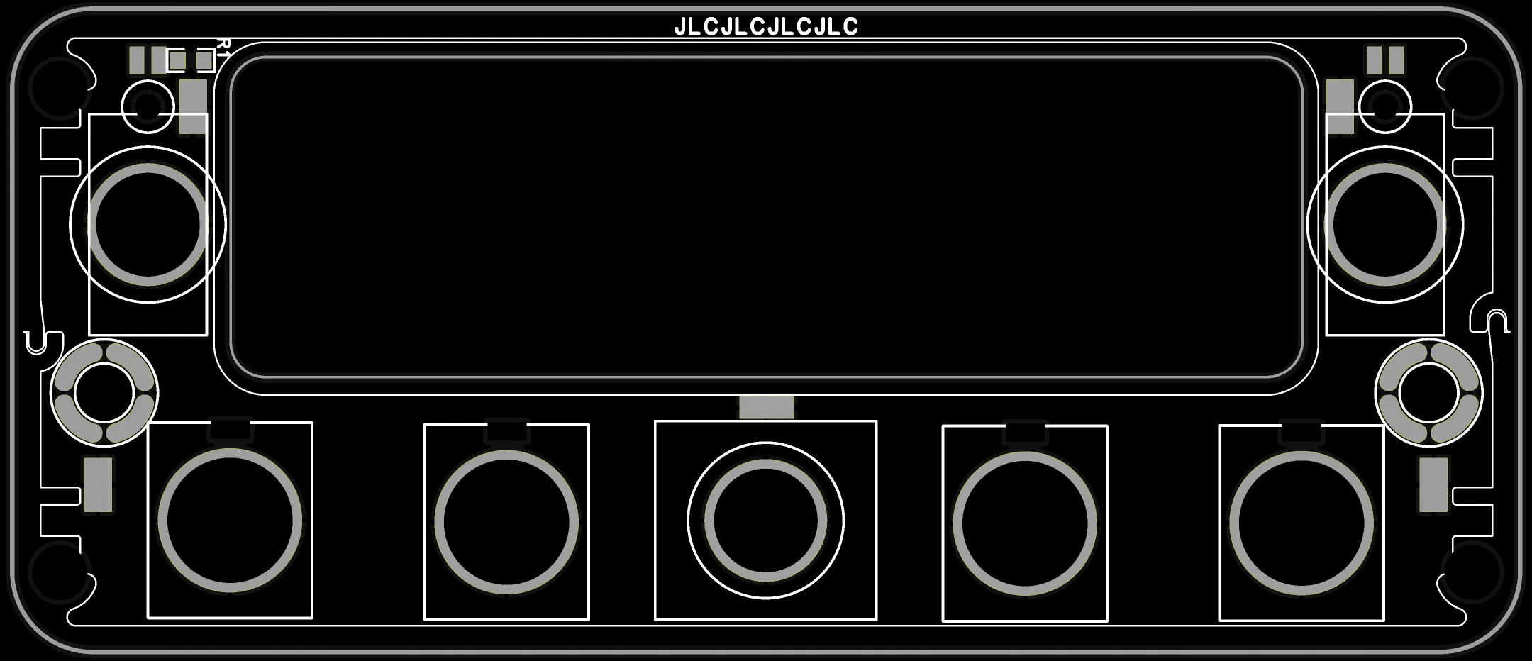
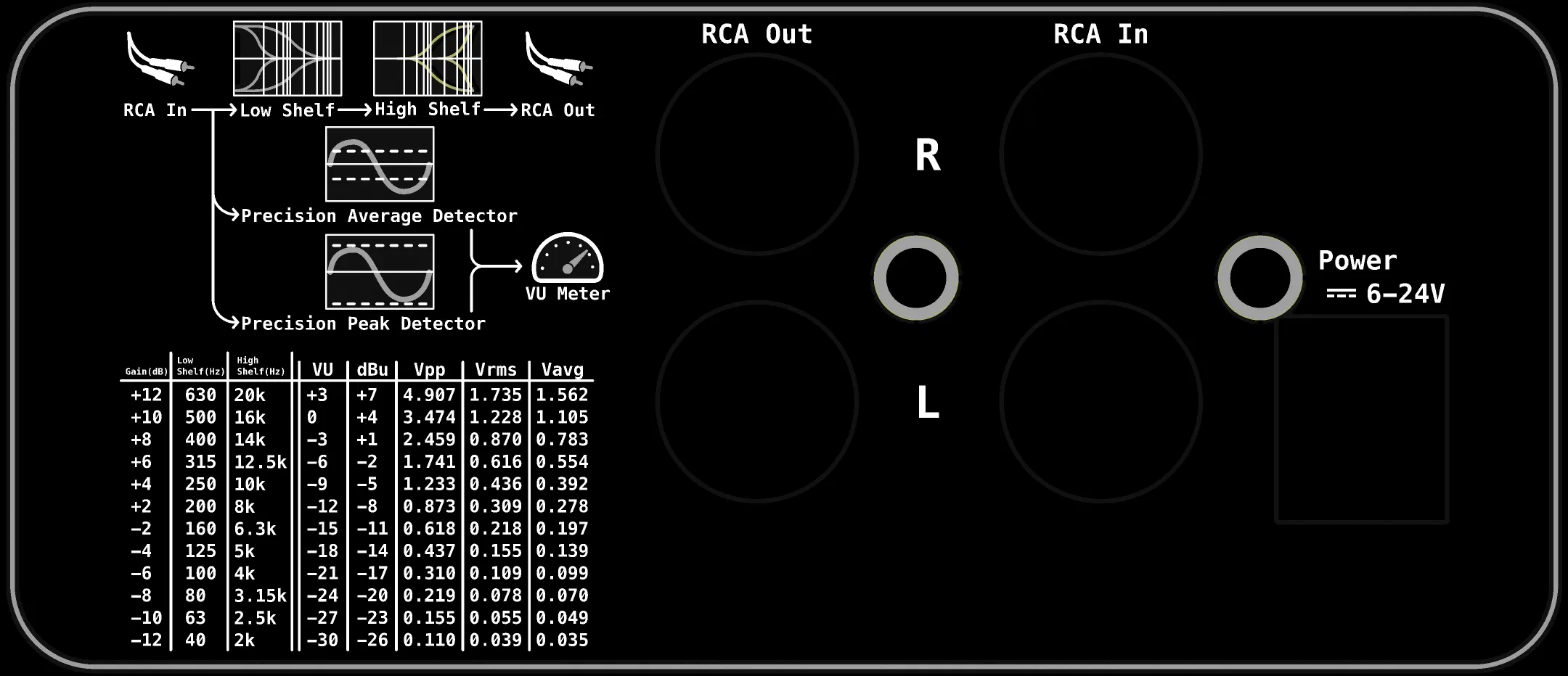
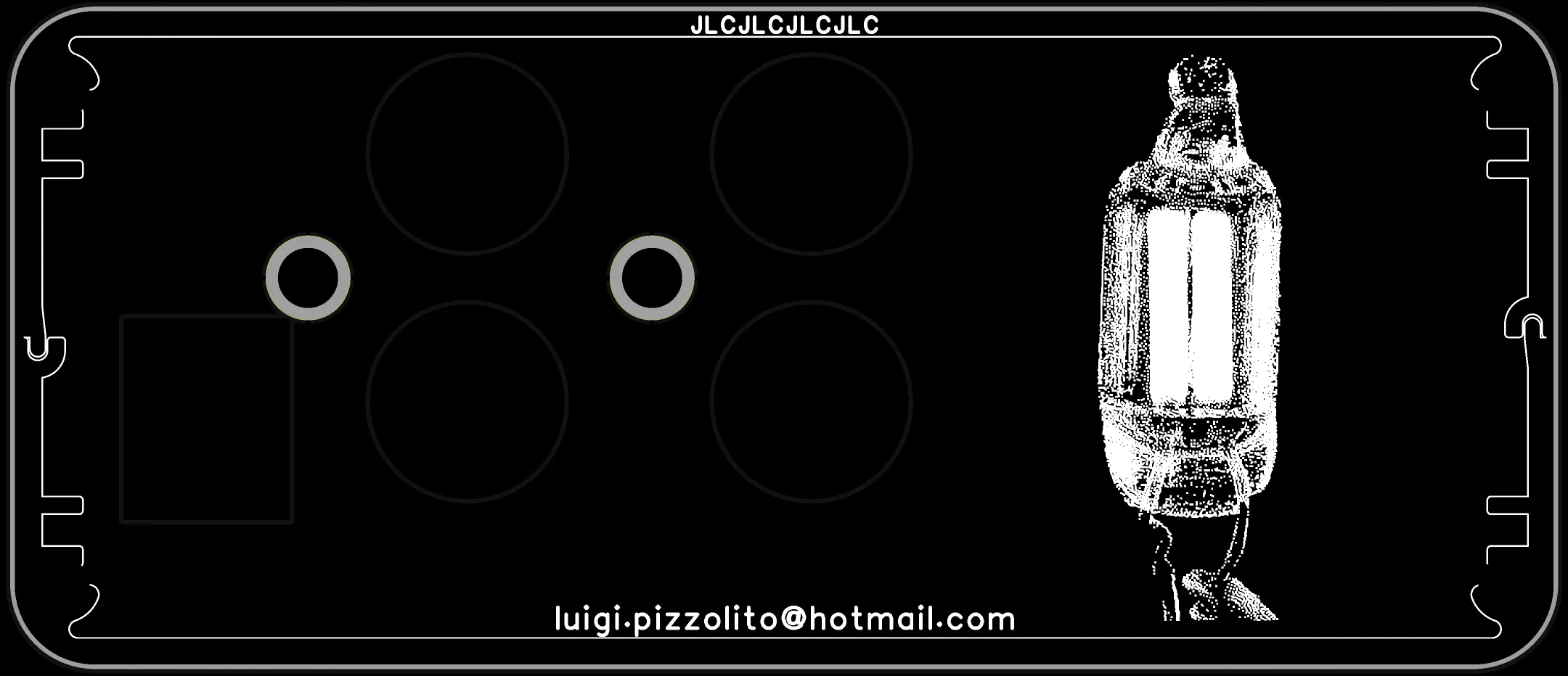
I took a lot of care to decorate and carefully design all of the silkscreen for an elegant and functional panel. As well as redesigning a logo for LPWorks for my audio-related projects (coincidentally, also modelled after a neon lamp).
To hold all of the neon lamps in place, I designed a custom piece which the lamps can be mounted to while having their leads passed through to the back. This piece needed to be SLA resin 3D printed due to the thin 0.8mm walls. I also designed some spacers to keep the potentiometers from rotating when panel-mounting them as the main PCB is not there to do that.
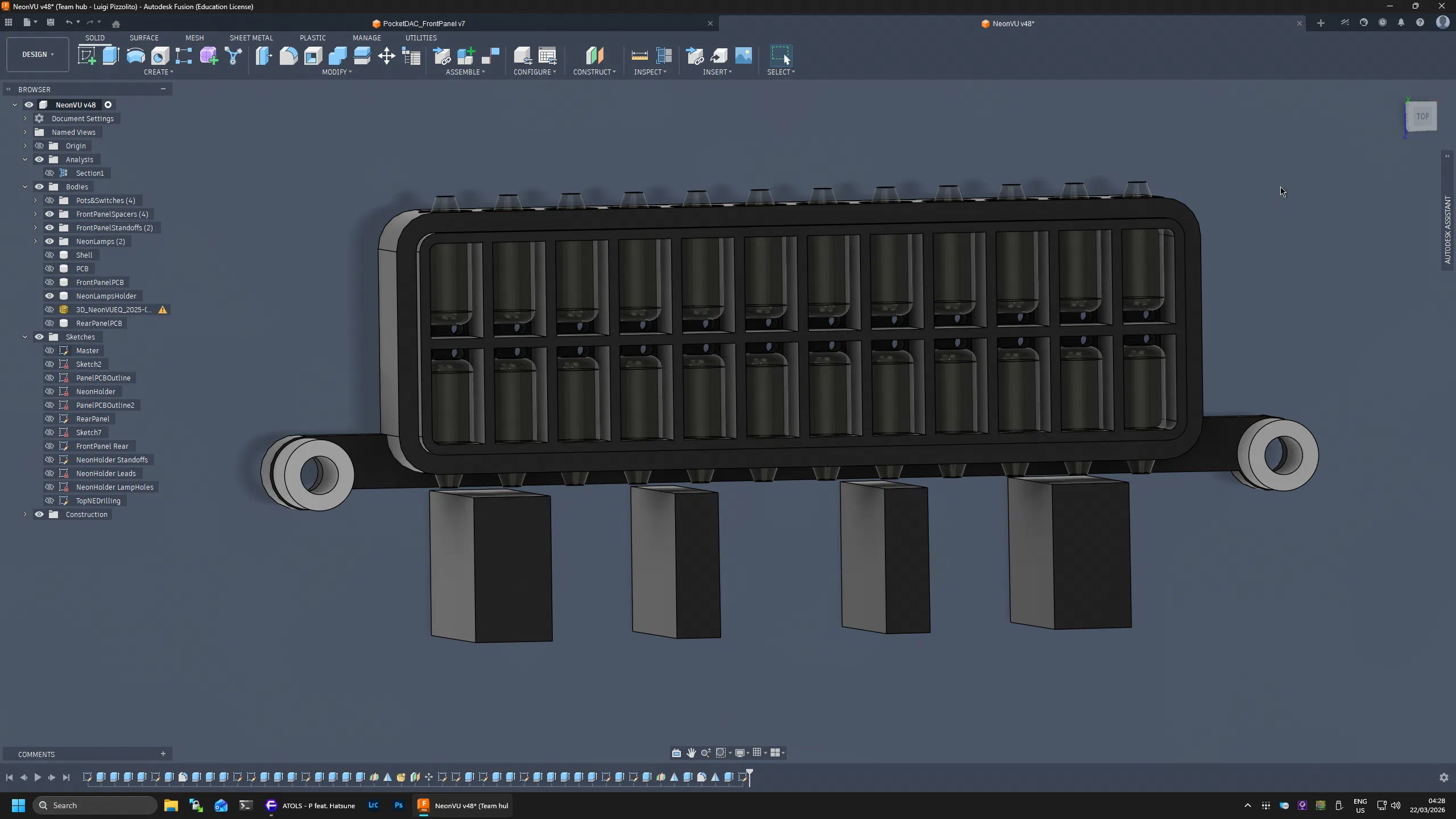
The neon holder piece was then secured to the back of the front panel PCB using some SMT M3 stand-offs. Another neat advantage of using PCBs for panels, allowing me to use this niche technique for a solid mount without anything visible from the front panel side.
First Prototype
To play around with the digital VU display and control interface code, I decided to first assemble just the analog EQ part of the circuit board and then prototype on breadboard the digital part using LEDs to finalise the MCU firmware. To do this I used a little CH32V003 breakout board and some wire wrapped connections to the peak and average analog outputs for one channel.
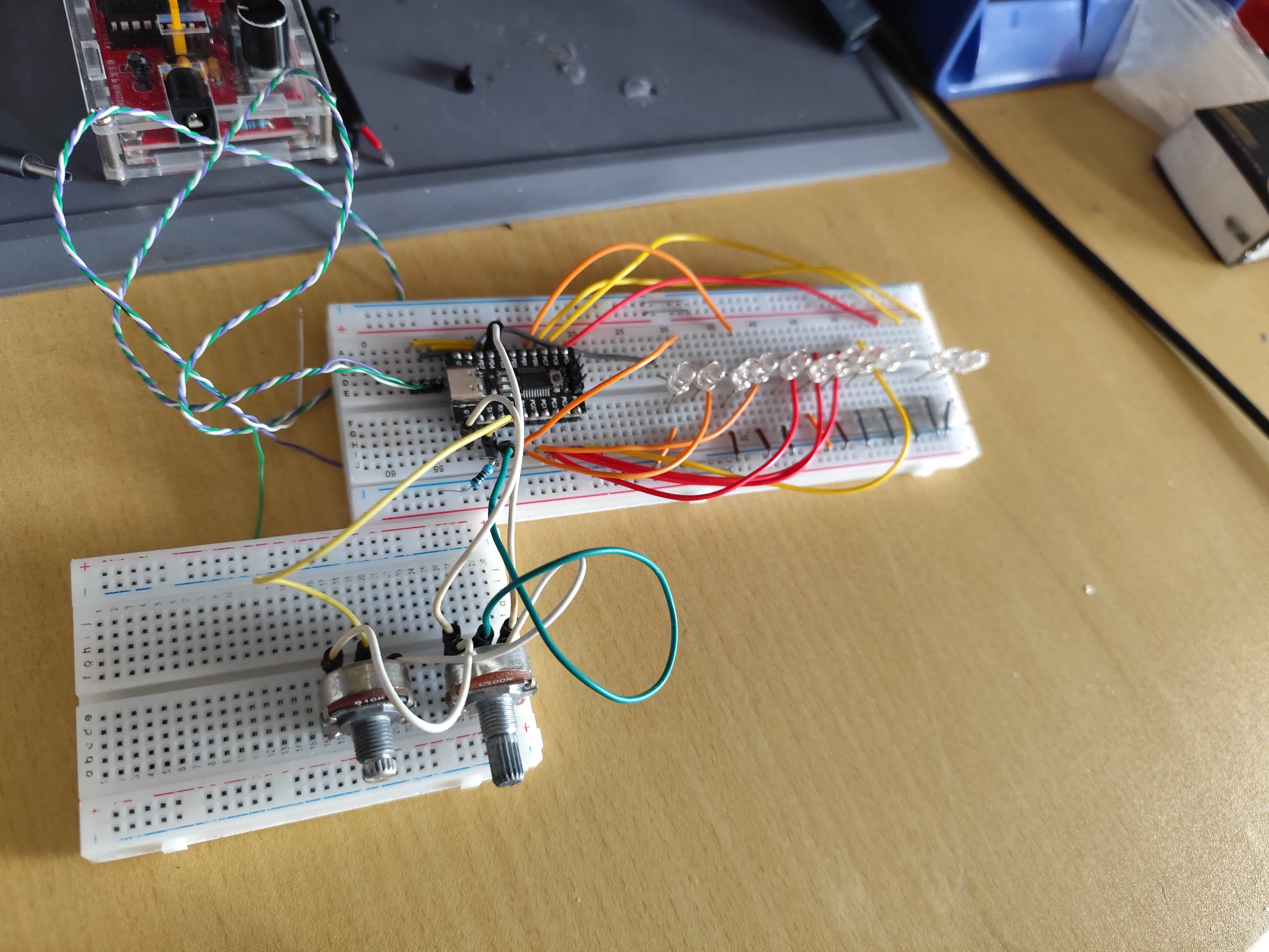
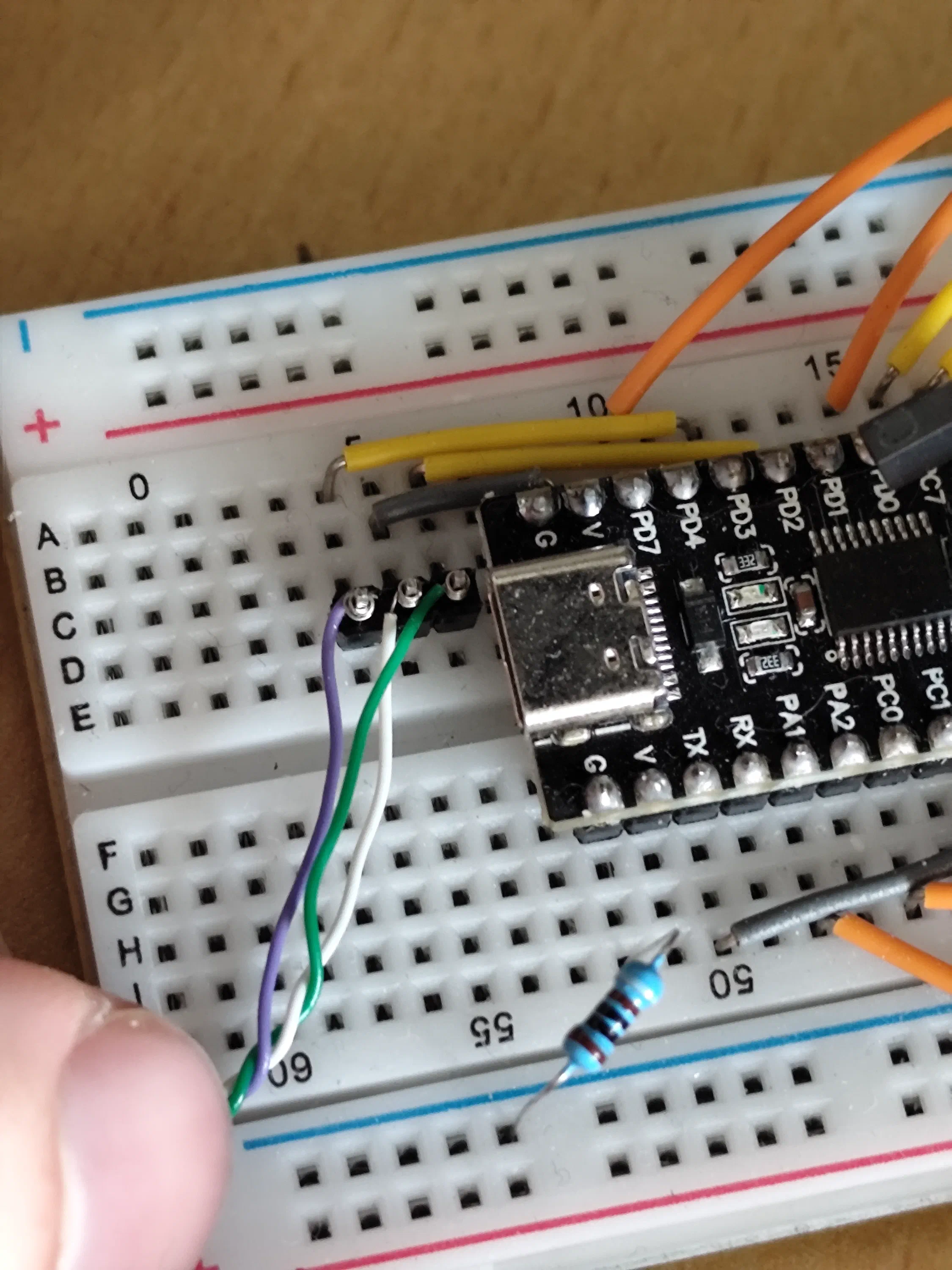
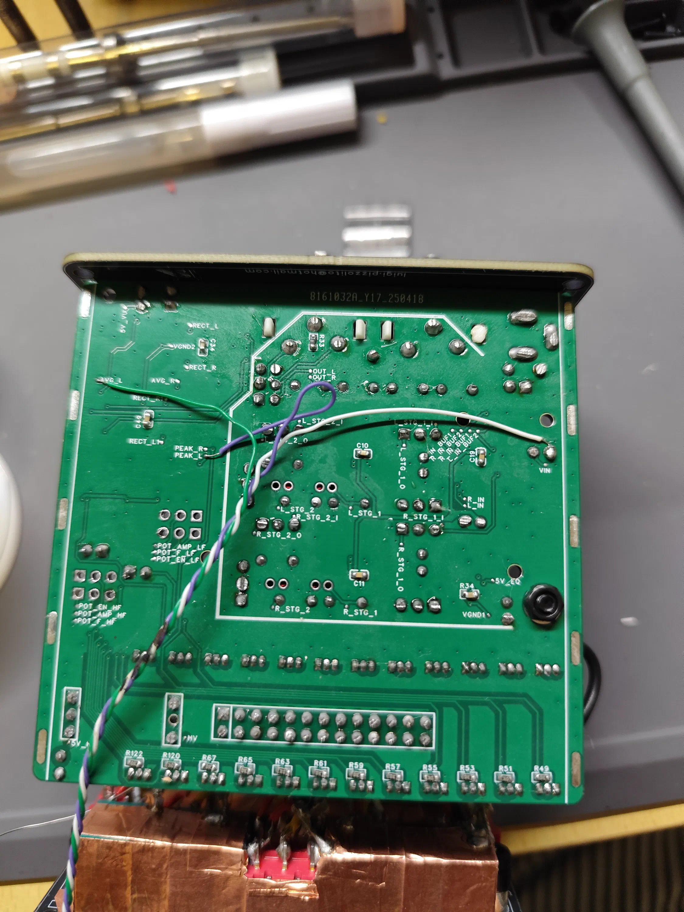
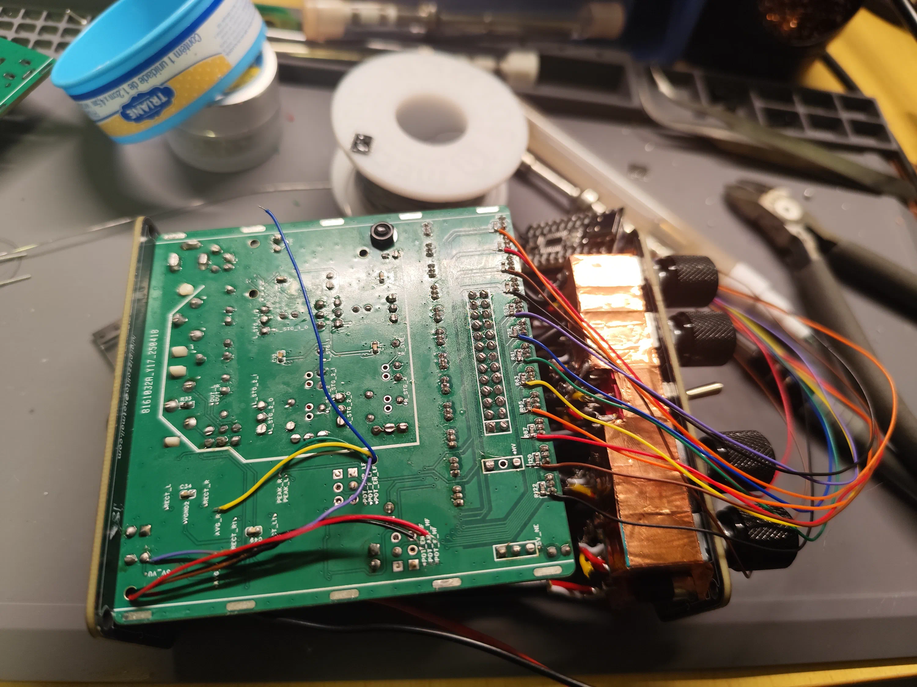
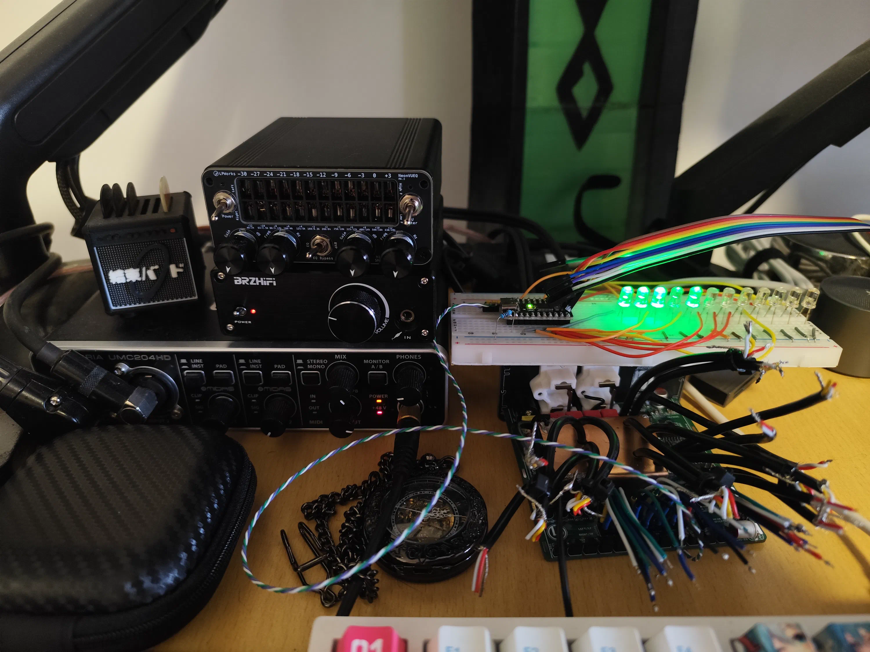
Notably, after the LED display on the prototype was working nicely, I also did a full test soldering all of the driver signals to the neon BJT drivers to see how the display would behave when using the real neon lamps.
MCU Programming
The programming for the CH32V003 is done in embedded C using ch32fun as I stated before. To facilitate it I created several mini header-only classes. rev_log_to_lin.h to convert the reverse log potentiometer ADC readings to a linear scale, pot_watch.h to watch the potentiometer values and trigger a function call if its detected that the potentiometers were moved, display.h to convert the measured ADC levels for the peak and average signals into the VU scale and composite them into display PWM outputs, and systick.h to enable more advanced system tick timers fo this MCU.
Reverse-Log Potentiometer Readings to Linear
The first issue to solve is that since we are reading the potentiometer positions using a simple voltage divider setup, and the potentiometers for frequency selection have reverse-logarithmic tapers; we need to unmap that from out ADC readings back into linear space to be able to display the selected frequency on the VU display. I implemented this with a 12-row look-up table (LUT) and linear interpolation for all the points in between:
 6typedef struct {
 7    uint16_t in;
 8    uint16_t out;
 9} MapPoint;
10
11uint16_t map_log_to_linear(uint16_t input) {
12    static const MapPoint table[] = {
13        {   0,   0},
14        {  90,  85},
15        { 317, 171},
16        { 430, 256},
17        { 553, 341},
18        { 760, 426},
19        { 844, 512},
20        { 871, 597},
21        { 900, 682},
22        { 927, 767},
23        { 963, 853},
24        {1010, 938},
25        {1023, 1023},
26    };
27    const int size = sizeof(table) / sizeof(table[0]);
28
29    if (input <= table[0].in) return table[0].out;
30    if (input >= table[size - 1].in) return table[size - 1].out;
31
32    for (int i = 0; i < size - 1; i++) {
33        if (input >= table[i].in && input <= table[i + 1].in) {
34            uint16_t in0 = table[i].in;
35            uint16_t out0 = table[i].out;
36            uint16_t in1 = table[i + 1].in;
37            uint16_t out1 = table[i + 1].out;
38
39            // Linear interpolation
40            return out0 + (uint32_t)(input - in0) * (out1 - out0) / (in1 - in0);
41        }
42    }
43
44    return 0; // Should not reach here
45}
Potentiometer Watch Detector
Next was the potentiometer watch detector. In the normal mode, the display shows the VU levels, but when any knob is moved (gain or frequency) the display switches over to displaying the selected gain or frequency. After a timeout, it returns to VU meter display. With the top row of VU neons working for the Left channel VU and low-shelf parameters, while the lower row of neons displays the Right channel VU and high-shelf parameters. For this we define a minimum change threshold and then just apply some comparisons:
10// Potentiometer Watch Functions
11uint16_t last_f_pot = 0;
12uint16_t last_amp_pot = 0;
13#define POT_CHANGE_THRESH 40
14
15#define POT_EN PD4
16
17uint8_t pot_watch_check(uint16_t *f_pot, uint16_t *amp_pot) {
18	// ADC is 10-bit, so 0-1023
19	*f_pot &= 0x03FF;	// Mask to 10 bits
20	*amp_pot &= 0x03FF; // Mask to 10 bits
21	// printf("F_POT: %d, AMP_POT: %d\n", *f_pot, *amp_pot);
22	// Check if pots have changed
23	uint16_t f_pot_thresh_h = (last_f_pot < 1023 - POT_CHANGE_THRESH) ? last_f_pot + POT_CHANGE_THRESH : 1023;
24	uint16_t f_pot_thresh_l = (last_f_pot > POT_CHANGE_THRESH) ? last_f_pot - POT_CHANGE_THRESH : 0;
25	// TODO: apply averaging if needed?
26	if (*f_pot > f_pot_thresh_h || *f_pot < f_pot_thresh_l) {
27		last_f_pot = *f_pot;
28		return 1; // Frequency pot changed
29	}
30	uint16_t amp_pot_thresh_h = (last_amp_pot < 1023 - POT_CHANGE_THRESH) ? last_amp_pot + POT_CHANGE_THRESH : 1023;
31	uint16_t amp_pot_thresh_l = (last_amp_pot > POT_CHANGE_THRESH) ? last_amp_pot - POT_CHANGE_THRESH : 0;
32	if (*amp_pot > amp_pot_thresh_h || *amp_pot < amp_pot_thresh_l) {
33		last_amp_pot = *amp_pot;
34		return 2; // Amplitude pot changed
35	}
36	// No change
37	return 0; // No change
38}
VU PWM Display Driver
This is by far the most complicated part of the code. We need to manage the mapping of the neon driver pins for both the Left/Right channel MCU cases which is reversed, mapping of the linear peak and average levels to the log dB scale, and also manage the display compositing. The code actually supports two display driver modes; bitmap mode (no fading) and PWM mode (fading). In the bitmap mode, the neons are only driven on or off. For the PWM mode, I needed to write a high-performance PWM software driver that can handle 12 simultaneous PWM outputs and update at a high refresh rate; as the MCU does not have enough hardware PWM peripherals.
For the bitmap driver case, it’s quite simple:
42// Bitmap driver function
43static inline void display_bitmap(uint16_t level) {
44	// Draw bitmap to screen
45	level = level & 0x0FFF; // Mask to 12 bits
46							// LSB => NE_0, MSB => NE_11
47	for (int i = 0; i < 12; i++) {
48		if (level & (1 << i)) {
49			funDigitalWrite(NE_PINS[i], FUN_HIGH);
50		} else {
51			funDigitalWrite(NE_PINS[i], FUN_LOW);
52		}
53	}
54}
Then for the PWM driver case, I had to make several optimizations to get the real-time performance needed on this tiny MCU:
56// PWM Driver function
57#if defined(PWM_DRIVER) || defined(PWM_DRIVER_KNOB)
58static uint8_t pwm_counter = 0;
59
60__attribute__((always_inline)) static inline void display_pwm_yield() {
61	// static uint8_t pwm_counter = 0; // Static counter to track PWM cycle
62	// // Output PWM levels based on counter
63	// for (uint8_t i = 0; i < 12; i++) {
64	// 	funDigitalWrite(NE_PINS[i], pwm_counter < pwm_levels[i]);
65	// }
66	// // Increment counter and reset
67	// pwm_counter+=64;
68	// if (pwm_counter >= 255) {
69	// 	pwm_counter = 0; // Reset counter after reaching max value
70	// }
71
72	// advance by 64; wraps 192→0 automatically on overflow
73	pwm_counter += 32;
74
75	// copy into locals
76	uint8_t cnt = pwm_counter;
77	uint8_t const *lvl = pwm_chans;
78	uint8_t const *pin = NE_PINS;
79
80	uint8_t const pi = peak_index;
81	uint8_t peak_led   = (pi > 0 && pi <= 12) ? (pi - 1) : 0xFF;
82	uint8_t idx = 0;
83
84	// process 12 channels in 3 unrolled steps of 4
85	for (uint8_t i = 0; i < 12; i +=4) {
86		// funDigitalWrite(pin[0], cnt < lvl[0]);
87		// funDigitalWrite(pin[1], cnt < lvl[1]);
88		// funDigitalWrite(pin[2], cnt < lvl[2]);
89		// funDigitalWrite(pin[3], cnt < lvl[3]);
90		funDigitalWrite(pin[0], (idx == peak_led) | (cnt < lvl[0]));  idx++;
91		funDigitalWrite(pin[1], (idx == peak_led) | (cnt < lvl[1]));  idx++;
92		funDigitalWrite(pin[2], (idx == peak_led) | (cnt < lvl[2]));  idx++;
93		funDigitalWrite(pin[3], (idx == peak_led) | (cnt < lvl[3]));  idx++;
94		pin += 4;
95		lvl += 4;
96	}
97
98}
First, I defined this function as always_inline as a static inline void which ensures we always insert the function code in-place and avoid the overhead of actually doing a function call and jumping around with the program counter (PC). Next, I copy all of the input level variables into local const variables to avoid fetching during the PWM write cycle. Lastly the actual PWM output for loop is unrolled into 3 iterations, each driving 4 neon channels; this was experimentally found to have the highest performance over writing to all channels at once. Notice also, that the single peak neon is a hard overlay using an OR operation; the VU meter is a PWM gradient and then that single peak is added on top as a full 255 maximum brightness output. Advancing the PWM counter by 32 steps each iteration provided a good balance between flickery-ness of the output and a fast response rate without overflowing the CPU timing budget of the PWM loop.
Next we have some helper functions to do the linear to log dB mapping for both the average and peak ADC readings. These are simple if chains with the values calculated from the spreadsheet before and adjusted based on oscilloscope readings with calibrated input signals:
120uint8_t map_adc2VUind(uint16_t *adc) {
121	*adc &= 0x3FF; // Mask to 10 bits
122	//*adc -= 511; // Remove VGND offset
123
124	// dumb mapping for now, use binary search for better performance
125	if (*adc >= 832)
126		return 12; // +3
127	if (*adc >= 738)
128		return 11; // 0
129	if (*adc >= 672)
130		return 10; // -3
131	if (*adc >= 625)
132		return 9; // -6
133	if (*adc >= 592)
134		return 8; // -9
135	if (*adc >= 569)
136		return 7; // -12
137	if (*adc >= 552)
138		return 6; // -15
139	if (*adc >= 541)
140		return 5; // -18
141	if (*adc >= 532)
142		return 4; // -21
143	if (*adc >= 526)
144		return 3; // -24
145	if (*adc >= 522)
146		return 2; // -27
147	if (*adc >= 519)
148		return 1; // -30
149	return 0;	  // <= -33
150}
151
152uint8_t map_adc2VUPeakind(uint16_t *adc) {
153	*adc &= 0x3FF; // Mask to 10 bits
154	//*adc -= 511; // Remove VGND offset
155
156	// dumb mapping for now, use binary search for better performance
157	if (*adc >= 1015)
158		return 12; // +3
159	if (*adc >= 868)
160		return 11; // 0
161	if (*adc >= 764)
162		return 10; // -3
163	if (*adc >= 690)
164		return 9; // -6
165	if (*adc >= 638)
166		return 8; // -9
167	if (*adc >= 601)
168		return 7; // -12
169	if (*adc >= 575)
170		return 6; // -15
171	if (*adc >= 557)
172		return 5; // -18
173	if (*adc >= 544)
174		return 4; // -21
175	if (*adc >= 534)
176		return 3; // -24
177	if (*adc >= 528)
178		return 2; // -27
179	if (*adc >= 523)
180		return 1; // -30
181	return 0;	  // <= -33
182}
Note here that although this if chain performance was enough for this project, it’s generally not good coding practice for performance. If needed, I would have converted this code to use a binary tree search through this decision space for a more optimised implementation.
Then we have higher-level functions to handle the display in each of the three states; VU display, gain knob display, and frequency knob display. Starting the the most interesting one, the main VU display:
259void display_map_VU_pwm(uint16_t *avg, uint16_t *peak) {
260	*avg &= 0x03FF;	 // Mask to 10 bits
261	*peak &= 0x03FF; // Mask to 10 bits
262
263	int8_t segment = -1;
264	for (uint8_t i = 0; i < 12; i++) {
265		if (*avg < VU_THRESHOLDS[i+1]) {
266			segment = i;
267			break;
268		}
269	}
270
271	// Clear all PWM levels to 0
272	for (uint8_t i = 0; i < 12; i++) {
273		pwm_chans[i] = 0;
274	}
275
276	// Calculate fade factor (0 to 255) for smooth transition
277	if (segment > 0) {
278		uint16_t seg_start = VU_THRESHOLDS[segment];
279		uint16_t seg_end = VU_THRESHOLDS[segment + 1];
280		uint16_t seg_len = seg_end - seg_start;
281		uint8_t fade = (seg_len > 1) ? (uint8_t)(((uint32_t)(*avg - seg_start) * 255) / (seg_len - 1)) : 255;
282		// fade current segment
283		pwm_chans[segment] = fade;
284		// Fully on below segment
285		for (uint8_t i = 0; i < segment; i++) {
286			pwm_chans[i] = 255; // Full brightness for all segments below
287		}
288		// Overlay peak indicator bit
289		uint16_t peak_bit = map_adc2VUPeakind(peak);
290		uint8_t idx = __builtin_ctz(peak_bit);
291		if (idx < 12) {
292			pwm_chans[idx] = 255; // Set peak bit to full brightness
293			peak_index = idx; // Update peak index
294		}
295	}
296
297}
First we calculate which is the highest VU segment that should be turned on. Crucially this is the highest VU dB level that was actualy reached; performing an effective floor operation rather than rounding. Then after clearing all of the PWM values, we fill all of the segments less than that peak segment with full brightness (255 value) and perform a linear interpolation to fade the segment above the peak segment based on the percentage that was reached of the next higher VU level. Lastly, we overlay the peak indicator segment at full brightness as well to finish compositing the full display. This function merely prepares the values, then a separate rendering function is called to dispatch the actual PWM driver we went over above and actually display to the driver outputs.
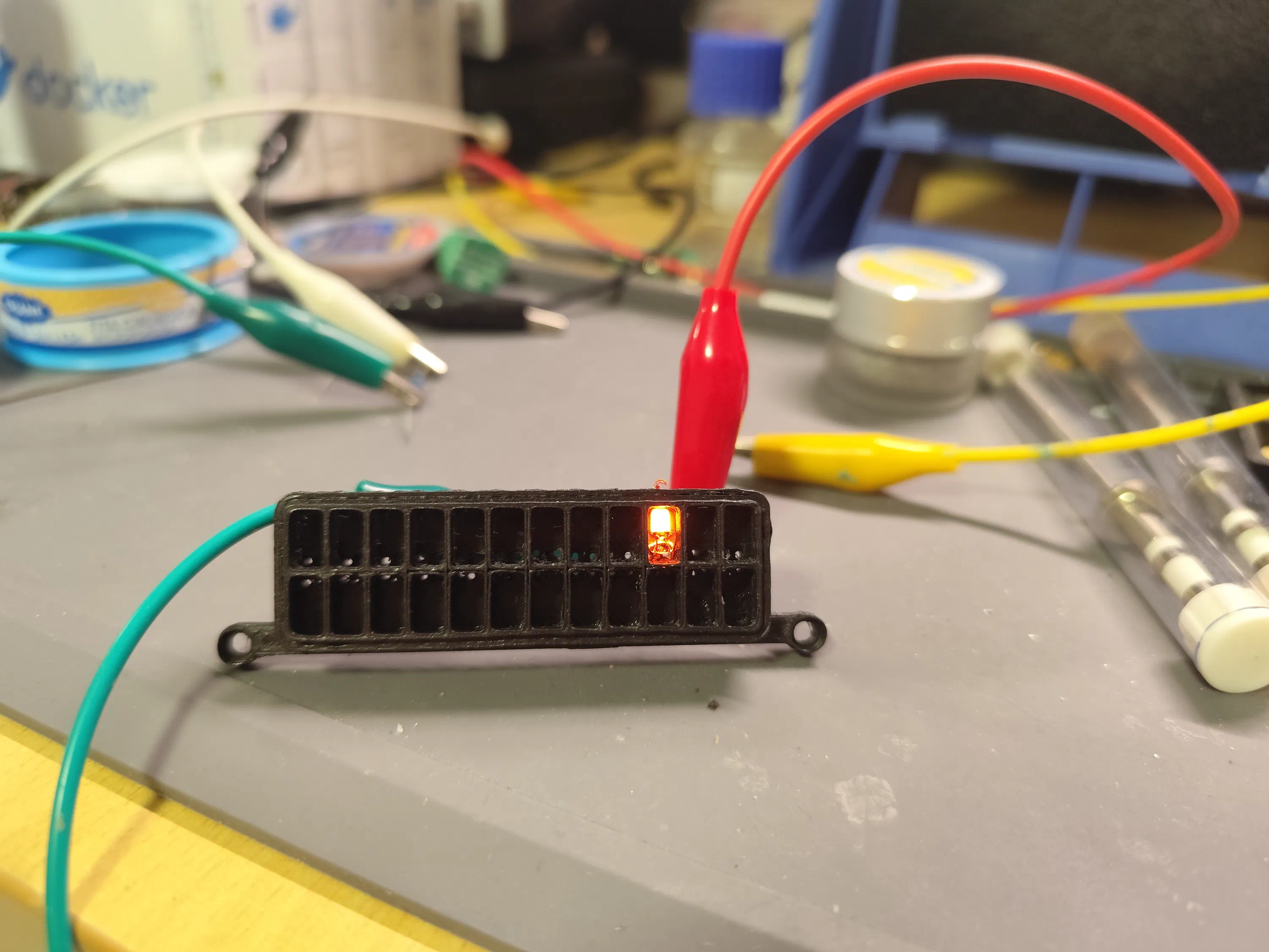
By having this PWM capability, not only can we more clearly distinguish between the average and peak levels, but also we obtain a much more analog feel, as the segments fade between each other rather than being hard thresholds like any digital LED VU meter. Surprisingly, the trigger (striking) time for small neon lamps is relatively short, which allows for very beautiful PWM fading; with the ionised neon gas itself providing smoothing with it’s residual glow.
Then, for the knob display modes, we have two simple functions that display gain and frequency in an intuitive way taking advantage of out PWM fading levels:
328void display_map_KNOB_amp_pwm(uint16_t *amp_pot) {
329	*amp_pot &= 0x03FF; // Mask to 10 bits
330	// Calculate position
331	// Calculate segment size for 12 lamps (1024 / 12 ≈ 85.33)
332    uint16_t segment_size = 1024 / 12;
333	// Find which segment the pot_value falls into (0 to 11)
334    uint8_t segment = *amp_pot / segment_size;
335    // Calculate position within the segment (0 to segment_size-1)
336    uint16_t position_in_segment = *amp_pot % segment_size;
337
338	// If pot_value is exactly at the max (1023), cap segment to 11
339    if (segment >= 12) {
340        segment = 11;
341        position_in_segment = segment_size - 1;
342    }
343
344	// Calculate fade factor (0 to 255) for smooth transition
345    uint8_t fade = (uint8_t)((position_in_segment * 255) / segment_size);
346
347	// Clear all PWM levels to 0
348    for (uint8_t i = 0; i < 12; i++) {
349        pwm_chans[i] = 0;
350    }
351
352	// Set the PWM level for the corresponding segments
353	// If not at the start of a segment, fade between two lamps
354    if (position_in_segment > 0 && segment < 11 && !(segment == 0 && position_in_segment < 16)) {
355        // Current lamp fades out, next lamp fades in
356        pwm_chans[segment] = 255 - fade;
357        pwm_chans[segment + 1] = fade;
358    } else {
359        // Light only the current lamp at full brightness
360        pwm_chans[segment] = 255;
361    }
362
363	// Fill from center out
364	if (segment <= 5) {
365		for (uint8_t i = 5; i > segment; i--) {
366			pwm_chans[i] = 255; // Set bits from level 0-6
367		}
368	} else if (segment >=6) {
369		for (uint8_t i = 6; i <= segment; i++) {
370			pwm_chans[i] = 255; // Set bits from level 7-11
371		}
372	}
373}
For the gain knob, since the range is from -12dB cut to +12dB boost, we indicated that by lighting all of the VU segments starting from the center up to the currently selected frequency. Additionally we apply some PWM fading with linear interpolation so that when the knob is in between two frequency points mapped to 2 VU segments, we proportionally fade in between the last two segments of the selection to offer a more precise pointer.
391void display_map_KNOB_freq_pwm(uint16_t *f_pot) {
392	*f_pot &= 0x03FF; // Mask to 10 bits
393	*f_pot = map_log_to_linear(*f_pot);
394	// Calculate position
395	// Calculate segment size for 12 lamps (1024 / 12 ≈ 85.33)
396    uint16_t segment_size = 1024 / 12;
397	// Find which segment the pot_value falls into (0 to 11)
398    uint8_t segment = *f_pot / segment_size;
399    // Calculate position within the segment (0 to segment_size-1)
400    uint16_t position_in_segment = *f_pot % segment_size;
401
402	// If pot_value is exactly at the max (1023), cap segment to 11
403    if (segment >= 12) {
404        segment = 11;
405        position_in_segment = segment_size - 1;
406    }
407
408	// Calculate fade factor (0 to 255) for smooth transition
409    uint8_t fade = (uint8_t)((position_in_segment * 255) / segment_size);
410
411	// Clear all PWM levels to 0
412    for (uint8_t i = 0; i < 12; i++) {
413        pwm_chans[i] = 0;
414    }
415
416	// Set the PWM level for the corresponding segments
417	// If not at the start of a segment, fade between two lamps
418    if (position_in_segment > 0 && segment < 11 && !(segment == 0 && position_in_segment < 16)) {
419        // Current lamp fades out, next lamp fades in
420        pwm_chans[segment] = 255 - fade;
421        pwm_chans[segment + 1] = fade;
422    } else {
423        // Light only the current lamp at full brightness
424        pwm_chans[segment] = 255;
425    }
426}
For the frequency knob, we don’t have this center-snap behaviour. Instead we just light up at most two VU segments at once, fading in between them as the knob is moved.
Lastly, we have a little helper function that perform a running-average on the ADC inputs. This is used during the start-up sequence to obtain the VMID bias point of the analog inputs. Although this should theoretically always be exactly 2.5V as the circuit we have for this virtual ground is generated by a 1/2 voltage divider from 5V; the real measurement can vary. Therefore we use this function to calibrate this on every boot:
476void calibrate_silence_offset() {
477	// Read the ADC values for VU_IN and PEAK_IN
478	uint16_t vu = GPIO_analogRead(GPIO_Ain3_D2);   // VU_IN
479	uint16_t peak = GPIO_analogRead(GPIO_Ain4_D3); // PEAK_IN
480	// Keep running average
481	cal_off_avg = (cal_off_avg + vu) / 2;
482	cal_off_peak = (cal_off_peak + peak) / 2;
483}
Main
Moving on to the main sketch, we start by defining a few configuration constants and importing those header-only libraries we created:
 3#include "ch32fun.h"
 4#include <stdio.h>
 5#include <stdlib.h>
 6
 7#include "ch32v003_GPIO_branchless.h"
 8#include "systick.h"
 9
10// Hardware options
11// #define RIGHT_CHANNEL_UNIT
12#ifndef RIGHT_CHANNEL_UNIT
13// Left channel unit
14#undef REVERSED_PINS
15#else
16// Right channel unit
17#define REVERSED_PINS
18#endif
19
20#define PWM_DRIVER
21
22#include "display.h"
23#include "pot_watch.h"
24#include "vu.h"
25
26enum display_mode {
27	MODE_VU = 0,
28	MODE_FREQ,
29	MODE_AMP,
30};
31enum display_mode current_mode = MODE_VU;
32
33#define KNOB_MODE_TIMEOUT 2000 // 2 seconds
34
35#define PWM_DRIVER
36#define KNOB_CHECK_INTERVAL 50 // 50ms/20Hz
37#define VU_CHECK_INTERVAL 25  // 10ms/100Hz
Then we proceed in our main function to initialise all of the peripherals and calibrate the silence VMID voltage offset:
 91int main() {
 92	SystemInit();
 93	printf("NeonVUEQ V0.1\n");
 94	printf("LPWorks 2025\n");
 95	// Initialize systick
 96	printf("initializing systick...\n");
 97	// ! Note, this breaks normal delay function, use delay_ms instead
 98	systick_init();
 99
100	printf("initializing GPIO...\n");
101	// Enable IO ports
102	GPIO_portEnable(GPIO_port_A);
103	GPIO_portEnable(GPIO_port_C);
104	GPIO_portEnable(GPIO_port_D);
105	// Set pin modes
106	// -- Analog inputs, PD2 VU_IN, PD3 PEAK_IN, PD6 F_POT, PD5 AMP_POT
107	GPIO_pinMode(GPIO_port_D, 2, GPIO_pinMode_I_analog, GPIO_SPEED_IN);
108	GPIO_pinMode(GPIO_port_D, 3, GPIO_pinMode_I_analog, GPIO_SPEED_IN);
109	GPIO_pinMode(GPIO_port_D, 5, GPIO_pinMode_I_analog, GPIO_SPEED_IN);
110	GPIO_pinMode(GPIO_port_D, 6, GPIO_pinMode_I_analog, GPIO_SPEED_IN);
111	// -- Display outputs, push-pull
112	for (int i = 0; i < 12; i++) {
113		funPinMode(NE_PINS[i], GPIO_CFGLR_OUT_10Mhz_PP);
114	}
115	// -- Pot EN
116	funPinMode(POT_EN, GPIO_CFGLR_OUT_10Mhz_PP);
117	funDigitalWrite(POT_EN, FUN_HIGH); // Enable pot
118
119	// Initialize ADC
120	printf("initializing ADC...\n");
121	GPIO_ADCinit();
122
123	printf("Calibrating silence offset...\n");
124	larson_test_and_calibrate();
125	printf("Offset avg: %d, peak: %d\n", cal_off_avg, cal_off_peak);
126
127	printf("Init done.\n");
Now for our main loop, we have an asynchronous section that completes the tasks needed to update the display at the update frequencies defined at the start of the sketch. Then after this, we call our display_pwm_yield(); function as fast as possible to run the PWM schedule for the display output.
Starting with the knob status display mode:
133 while (1) {
134
135
136 // Check display mode
137 if (current_mode > MODE_VU && KNOB_CHECK_INTERVAL > 0) {
138 // In freq/amp display mode
139 // printf("Current mode: %d\n", current_mode);
140 // Check if it is time to update the display
141 if (millis() - last_KNOB_update_time >= KNOB_CHECK_INTERVAL) {
142 // 0. Update timer
143 last_KNOB_update_time = millis();
144
145 // 1. Check if we have timed out, if so switch back to VU mode
146 if (millis() > pot_timeout) {
147 current_mode = MODE_VU;
148 printf("Timeout: Switching to VU mode\n");
149 pot_timeout = 0; // Reset timeout
150 continue; // Skip to next loop
151 }
152
153 // 2. Read knobs
154 uint16_t f_pot = GPIO_analogRead(GPIO_Ain6_D6); // F_POT
155 uint16_t amp_pot = GPIO_analogRead(GPIO_Ain5_D5); // AMP_POT
156 // 3. Switch to changed knob mode, but not VU_MODE
157 uint8_t new_mode = pot_watch_check(&f_pot, &_pot);
158 if (current_mode == MODE_FREQ && new_mode == MODE_AMP) {
159 current_mode = MODE_AMP;
160 printf("Switching to AMP mode\n");
161 } else if (current_mode == MODE_AMP && new_mode == MODE_FREQ) {
162 current_mode = MODE_FREQ;
163 printf("Switching to FREQ mode\n");
164 }
165 // 4. Reset timeout if knobs were moved
166 if (new_mode != 0) {
167 pot_timeout = millis() + KNOB_MODE_TIMEOUT;
168 }
169
170 // printf("MODE: %s, F_POT: %d, AMP_POT: %d\n", (current_mode == MODE_FREQ) ? "MODE_FREQ" : "MODE_AMP", f_pot, amp_pot);
171
172 // 5. Switch over knob display mode, and call display function
173 switch (current_mode) {
174 case MODE_FREQ:
175 // Display frequency knob
176 display_KNOB_freq(&f_pot);
177 break;
178 case MODE_AMP:
179 // Display amplitude
180 display_KNOB_amp(&_pot);
181 break;
182 default:
183 // Shouldn't happen
184 continue; // Skip to next loop
185 }
186 }It is pretty straight-forward, we just run the state machine to check if we should switch back to VU mode and if not we read the knobs and use the pot_watch library to check if we should switch modes accordingly. When we are actually in a knob display mode, we simply dispatch the corresponding display_KNOB function.
Then for VU display mode:
188 } else {
189 // In VU mode
190 // Check if it is time to update the display
191 if (millis() - last_VU_update_time >= VU_CHECK_INTERVAL) { // 100Hz refresh rate, max 800Hz ish (1250uS)
192
193 // 0. Update timer
194 last_VU_update_time = millis();
195 // uint32_t timer_start = micros();
196
197 // 1. Read ADCs, takes ~1.2ms
198 uint16_t vu = GPIO_analogRead(GPIO_Ain3_D2); // VU_IN
199 uint16_t peak = GPIO_analogRead(GPIO_Ain4_D3); // PEAK_IN
200
201 uint16_t f_pot = GPIO_analogRead(GPIO_Ain6_D6); // F_POT
202 uint16_t amp_pot = GPIO_analogRead(GPIO_Ain5_D5); // AMP_POT
203
204 // printf("VU_MODE: VU: %d, PEAK: %d, F_POT: %d, AMP_POT: %d\n", vu, peak, f_pot, amp_pot);
205
206 // 2. Check if knobs were moved
207
208 current_mode = pot_watch_check(&f_pot, &_pot);
209 // printf("Current mode: %d\n", current_mode);
210 if (current_mode != MODE_VU && millis() > KNOB_MODE_TIMEOUT*2) {
211 // Knob was moved, set inital timeout
212 pot_timeout = millis() + KNOB_MODE_TIMEOUT;
213 continue; // Skip VU update
214 }
215
216
217 // 3. Update VU display
218 display_VU(&vu, &peak);
219 // printf("VU Update took %d us out of %d us budget.\n", (micros() - timer_start),
220 // VU_CHECK_INTERVAL * 1000);
221 }
222 }We update our timers, take all four ADC readings, then after checking if the pots were moved we either switch the machine state or just call the display_VU function.
Lastly, yielding to the PWM display driver function:
225		// Yield for software PWM
226		#ifdef PWM_DRIVER
227			display_pwm_yield();
228		#endif
229
230
231	}
Below is my GitHub repository with all of the code, where you can check the full code and view further details. Such as the CH32V003 config and setup files and so on.
When I was satisfied with program, this was the final result when using LEDs for display:
Assembly
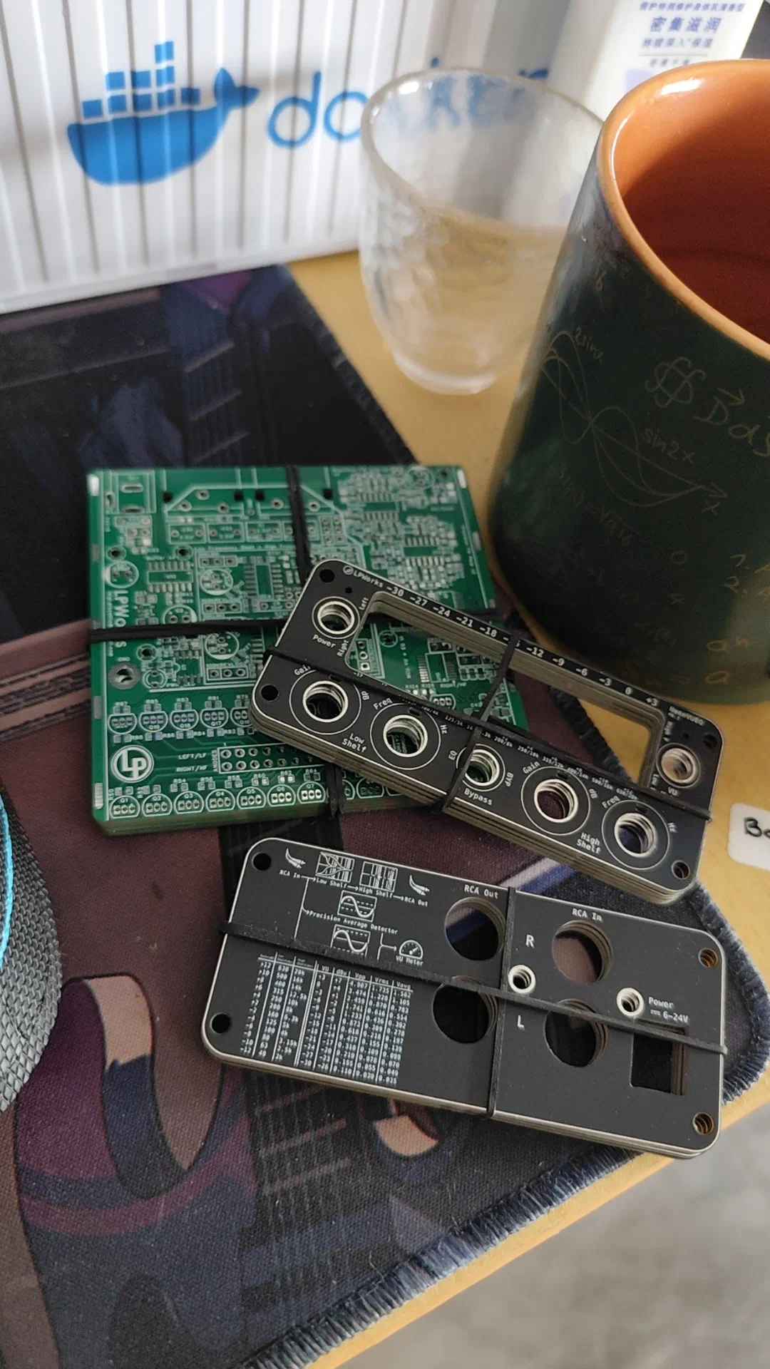
After all 3 boards and parts arrived, it was on with the long assembly process.
Board Assembly
I started by assembling and testing the analog EQ part of the board, including with the digital prototype shown above. After that testing was complete, I finished the entire board assembly.
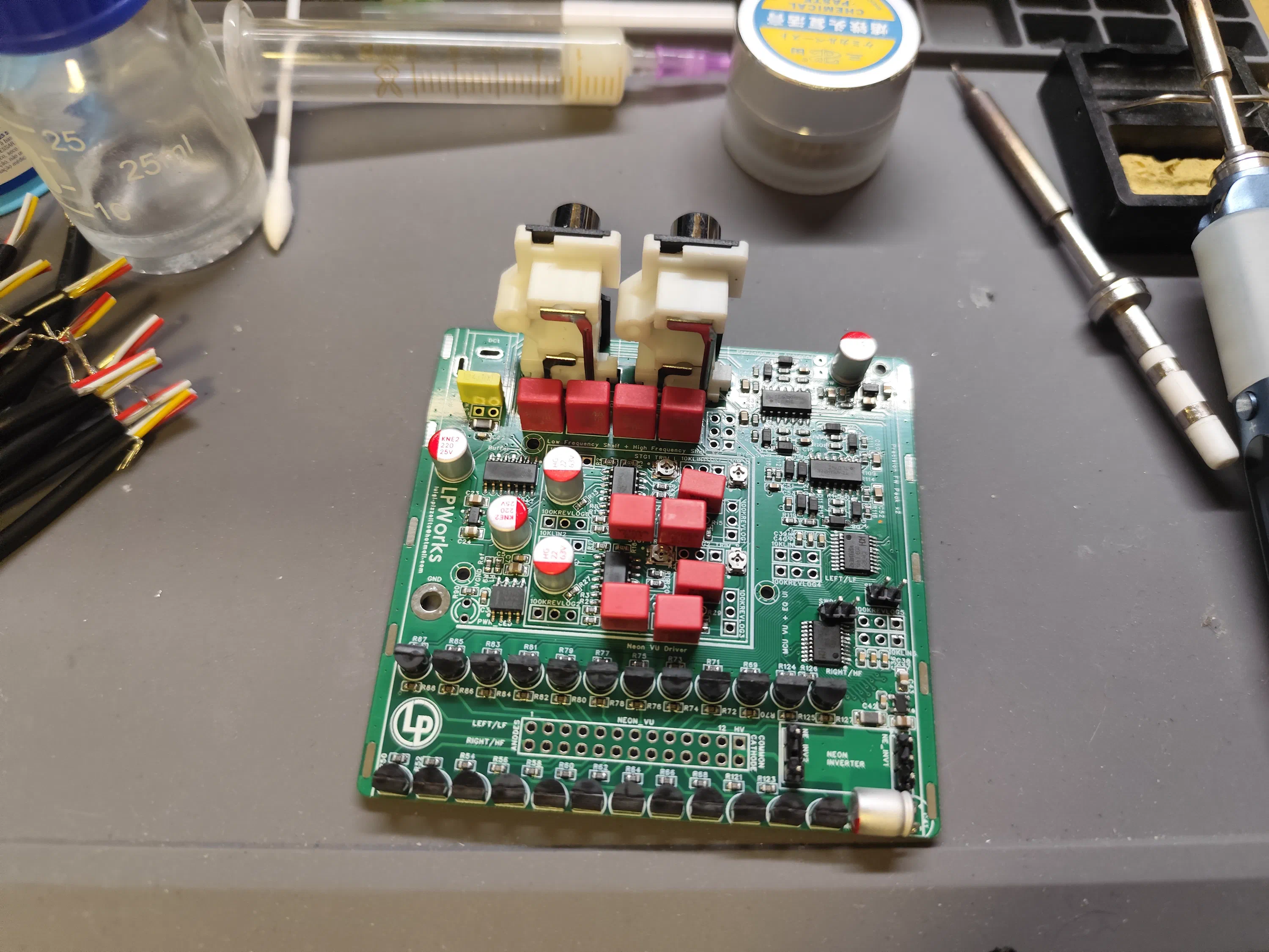
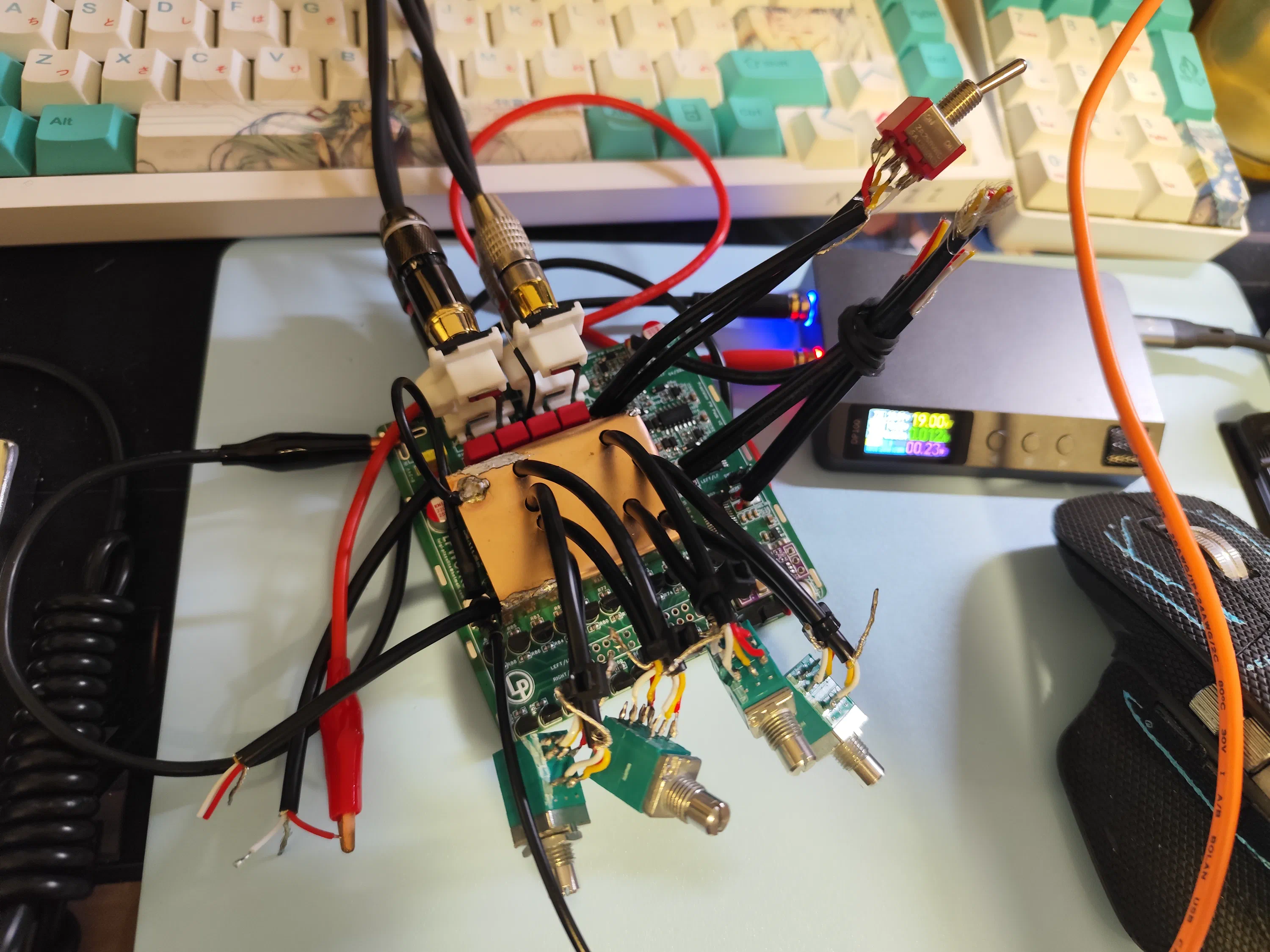
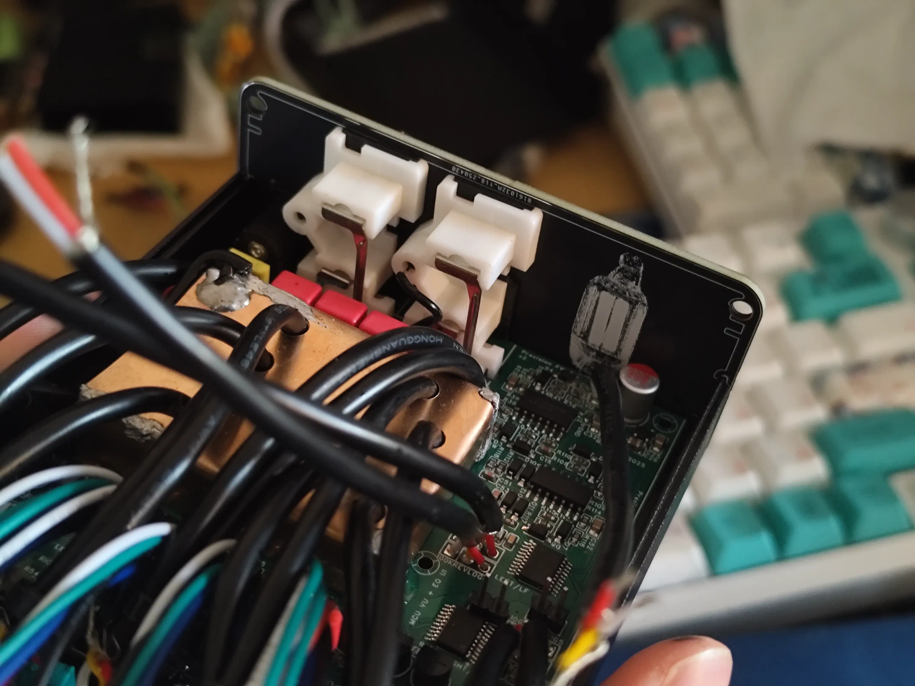
The next step was to prepare this copper RF shield for the analog section. Which I cut and bent myself from a copper sheet. Shielded 3-core wire was used for all of the potentiometer wiring as they would cary the analog audio signals and I did not want to pick up any interference from the HV sections.
Display Assembly
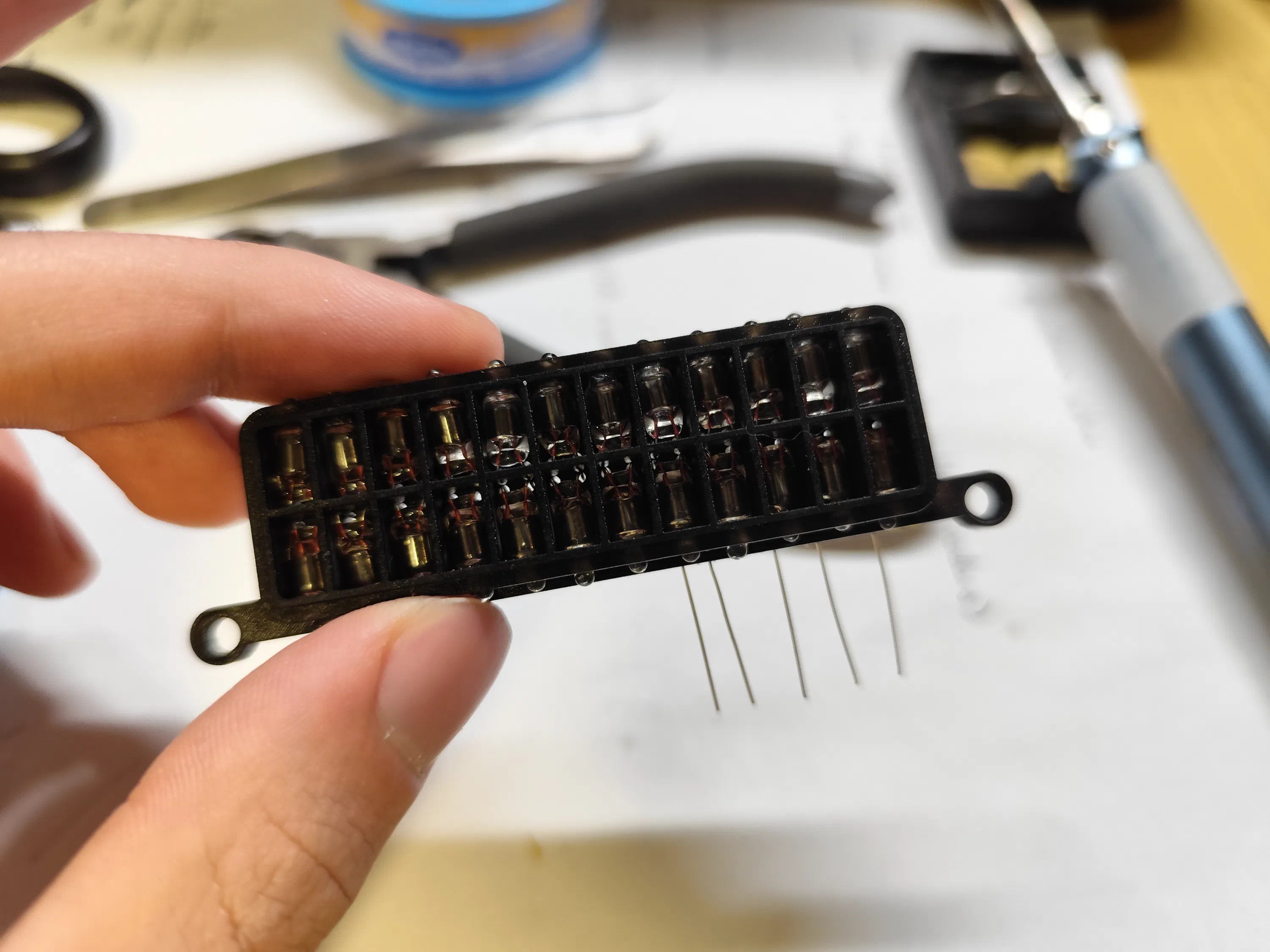
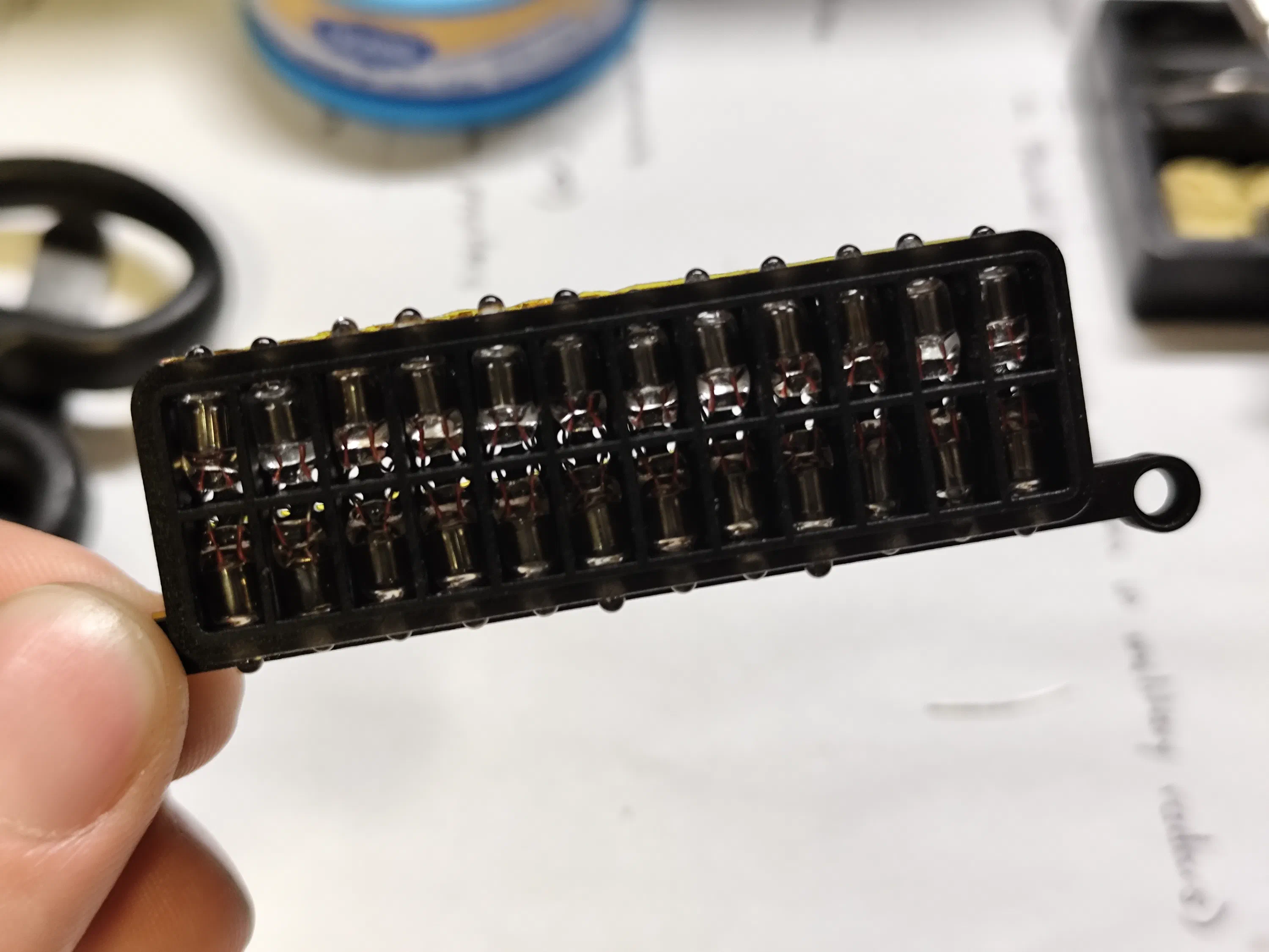
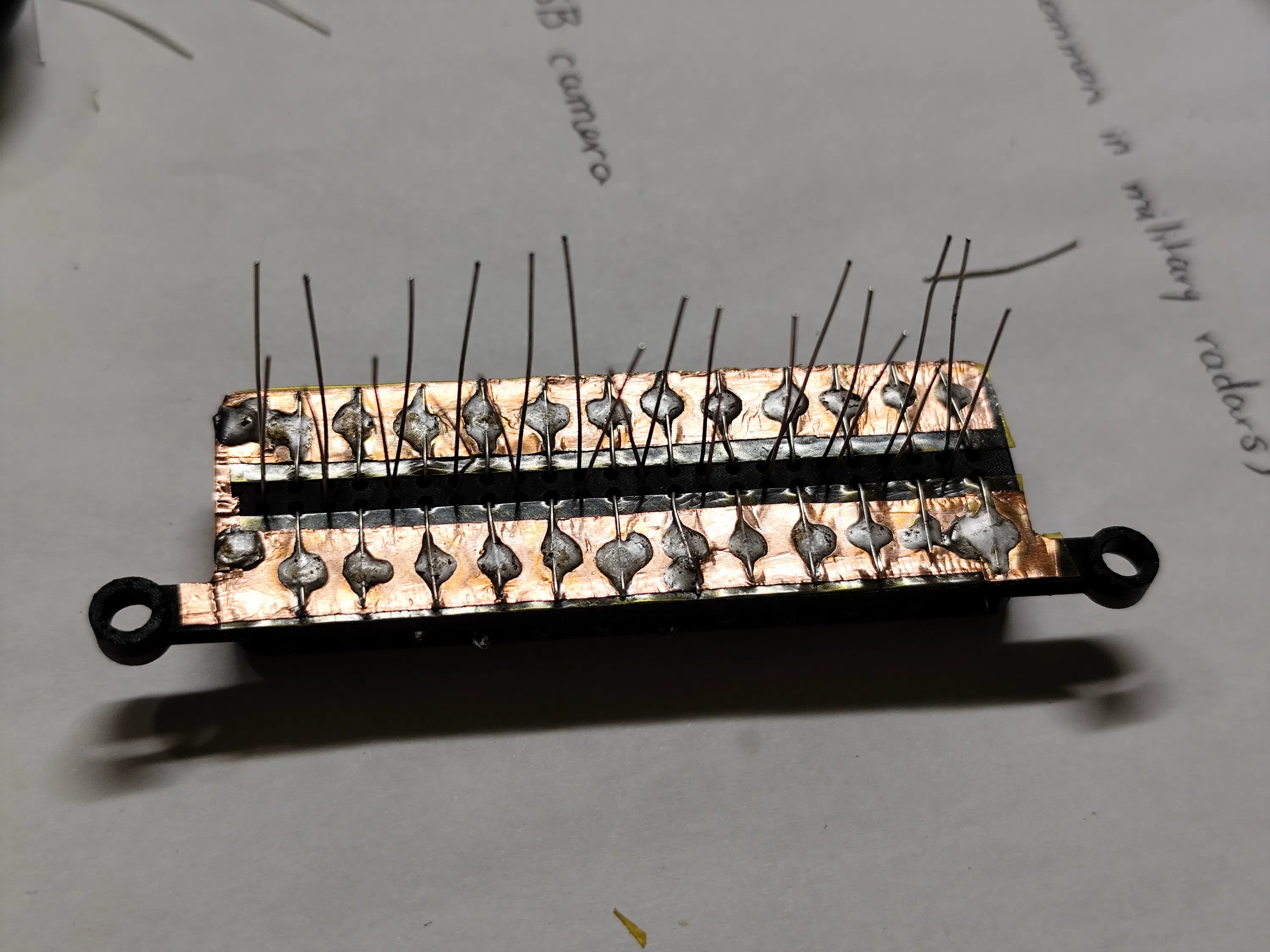
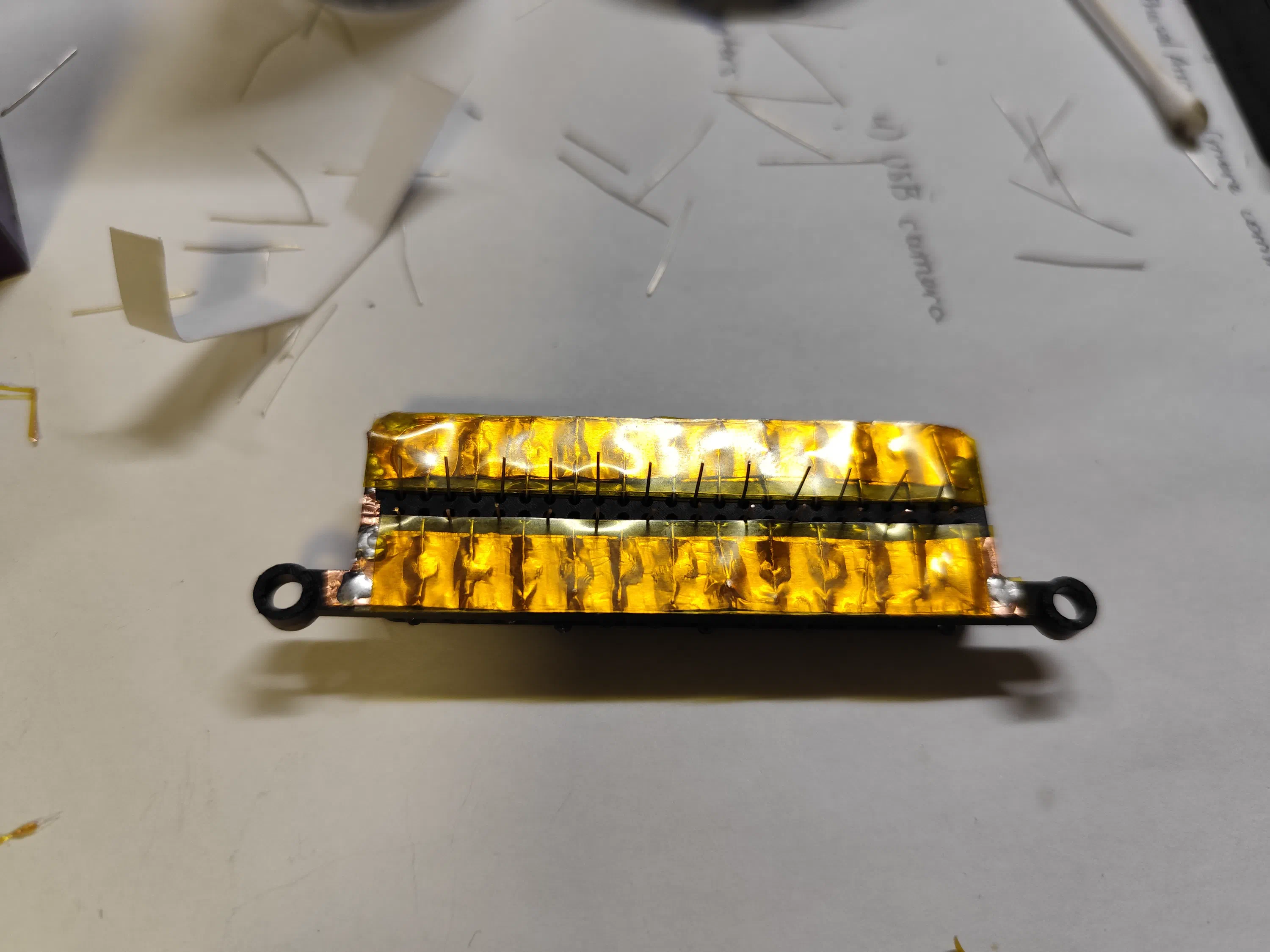
Next up was the display assembly. After receiving the SLA printed part from JLC3DP, I started by slotting all of the neon lamps inside with the leads pre-bent. After that, a combination of copper tape, solder, UV glue and Kapton tape was used to assemble the common cathode contacts at the back of the panel while leaving the individually driven anodes sticking out for soldering the drive wires.
Panel Assembly
With that sub-assembly complete, I continued by assembling everything into the front panel PCB.
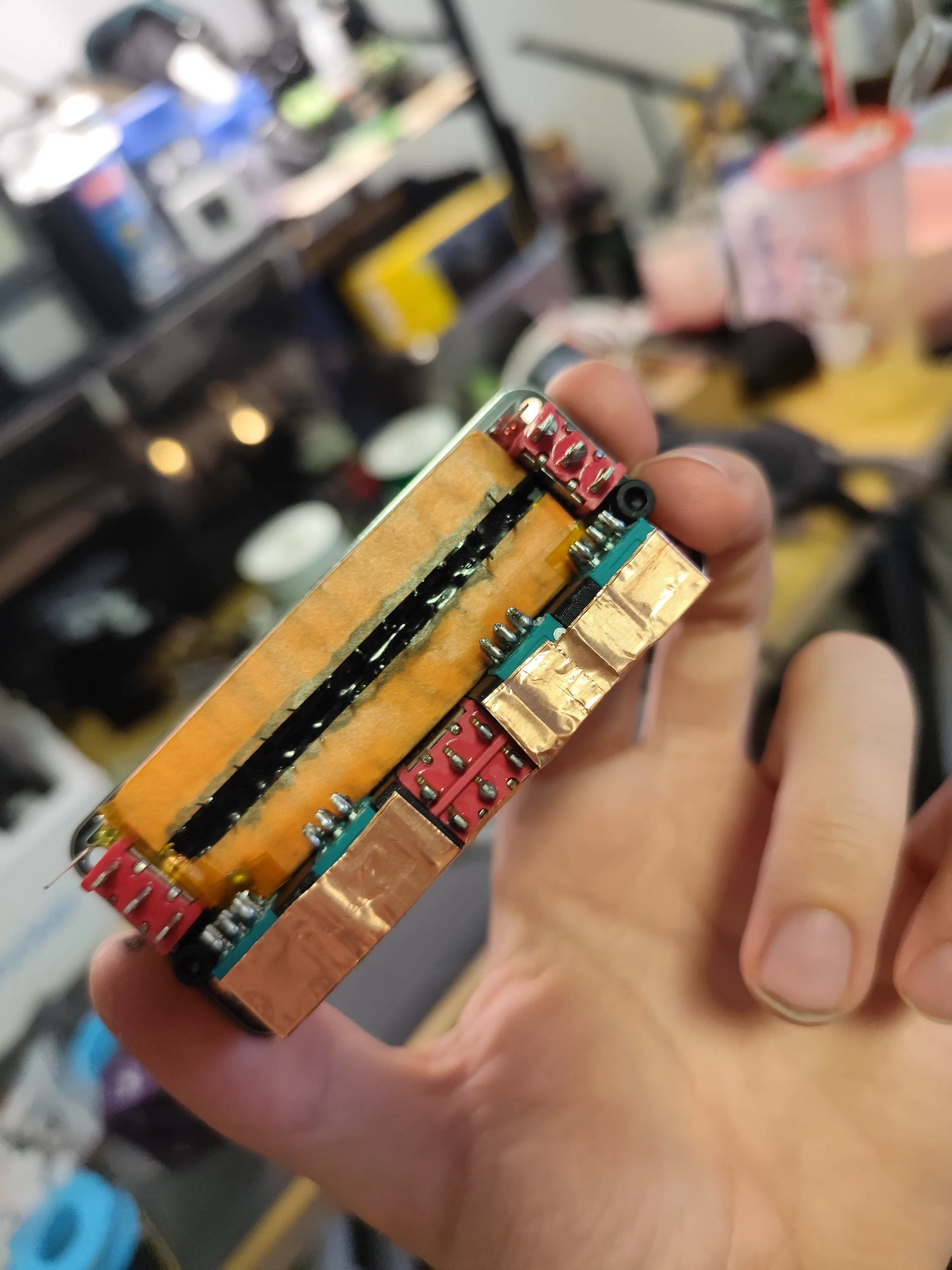
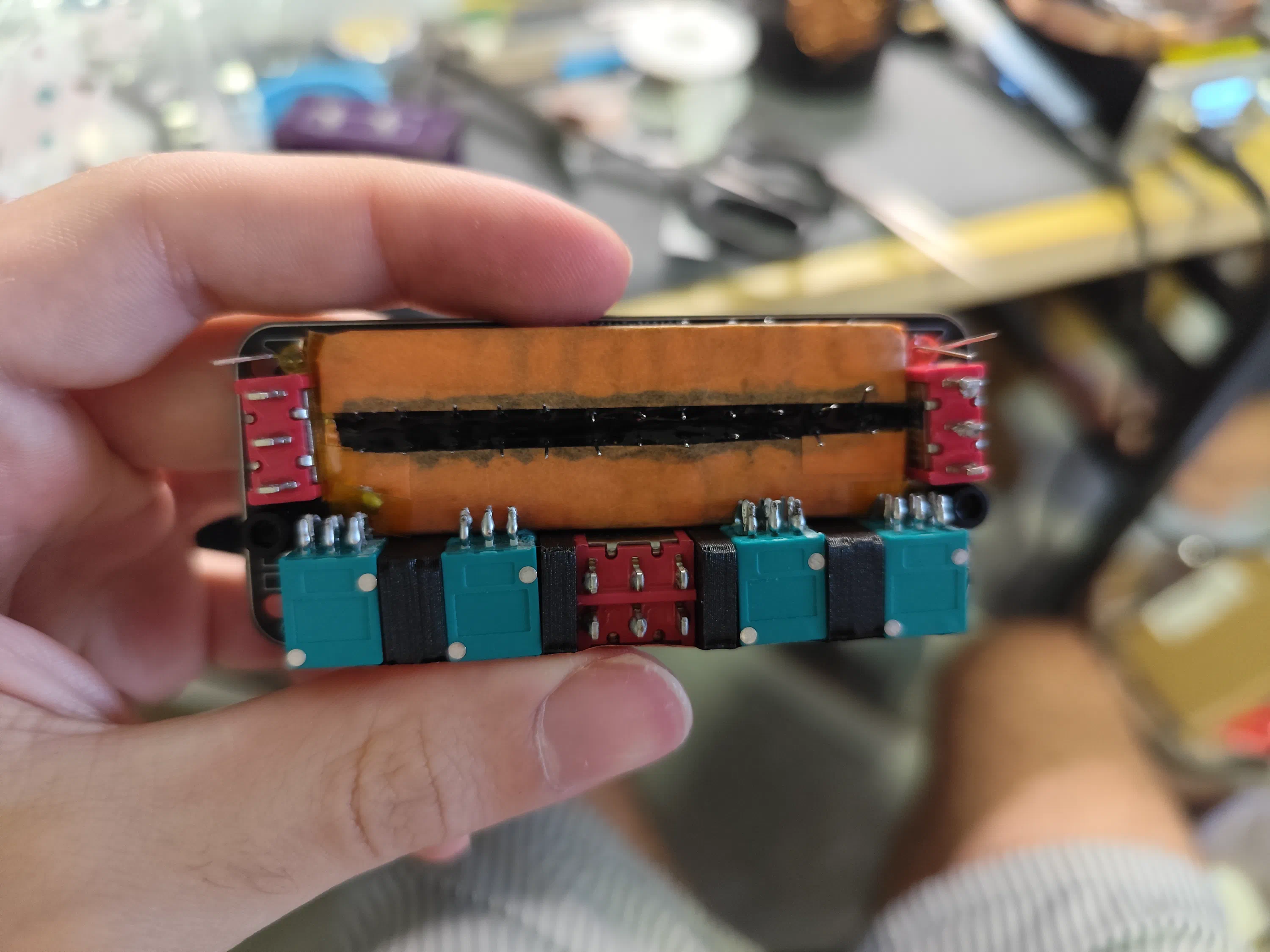
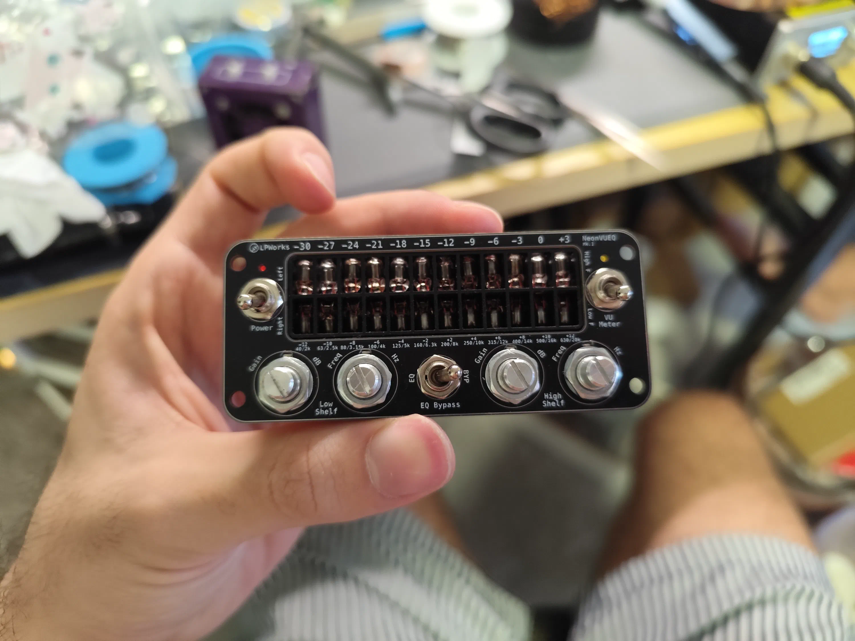
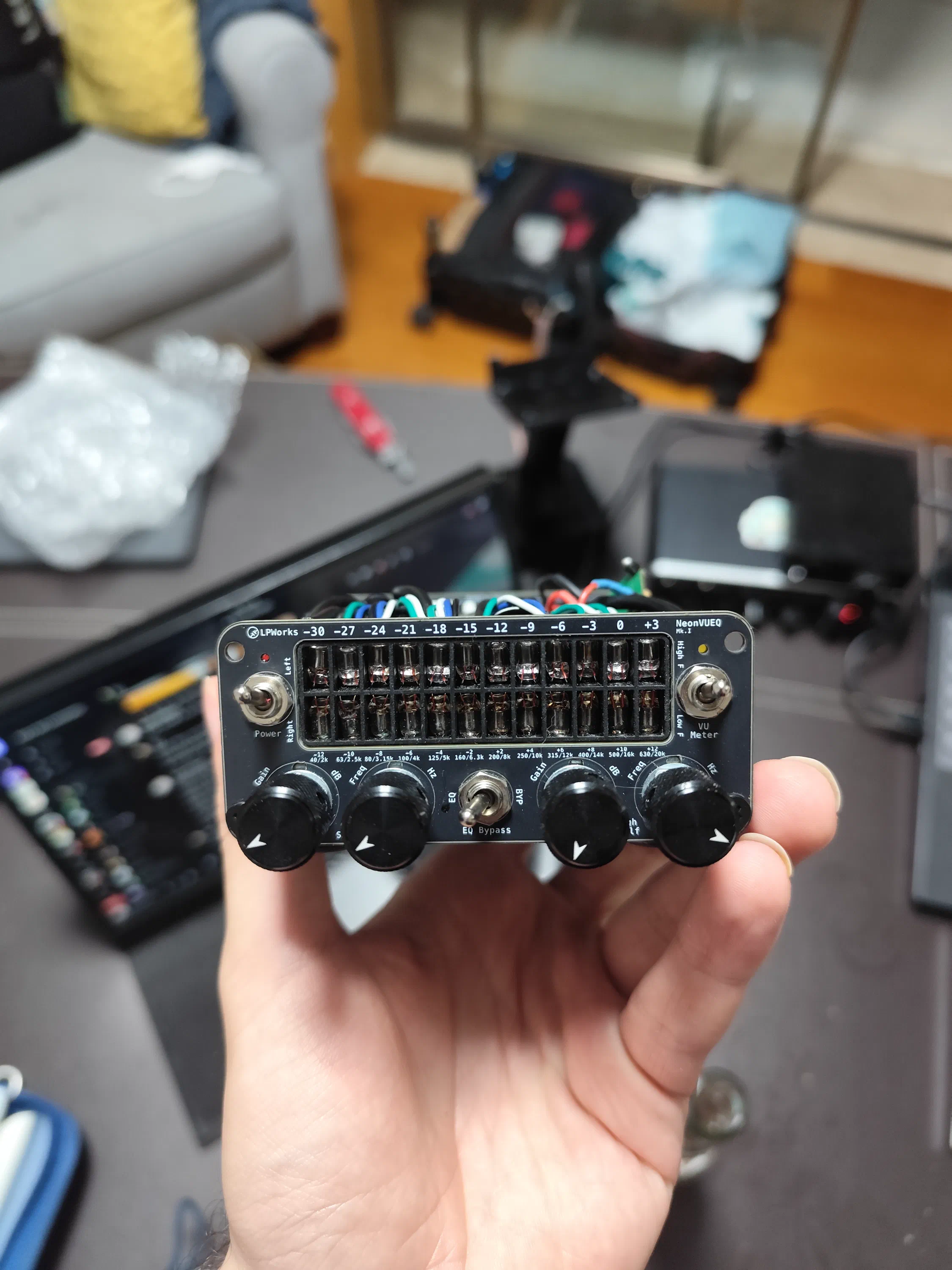
This was a real tight panel, with tolerances of 0.5mm at some parts. The large tactile switches and high-quality Alps Alpine potentiometer really took their space. I also added some more grounded copper tape around the pots to RF shield them. Next I continued taking many hours to do the painful process of preparing and soldering all of the wires from the front panel to the main PCB.
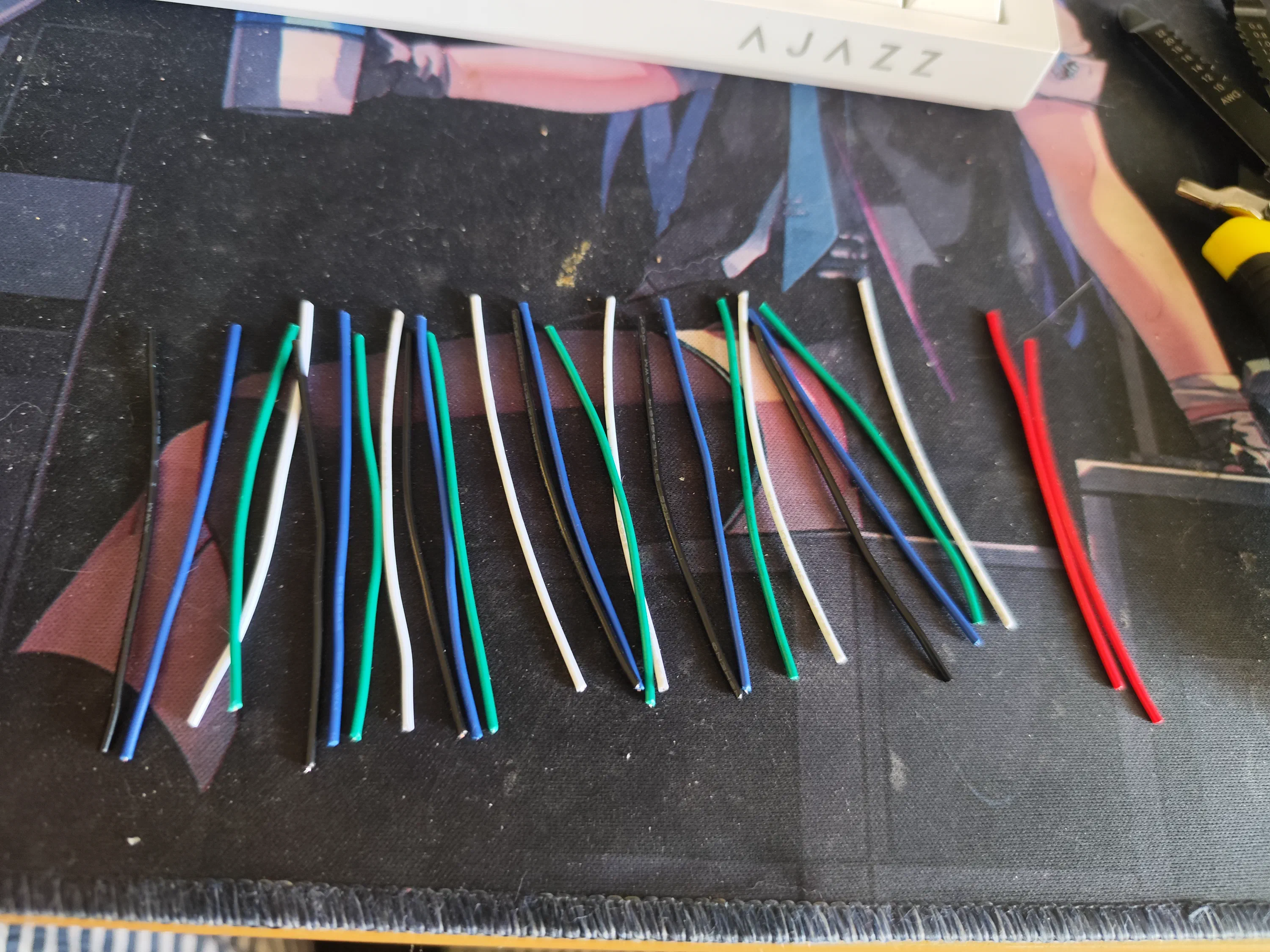
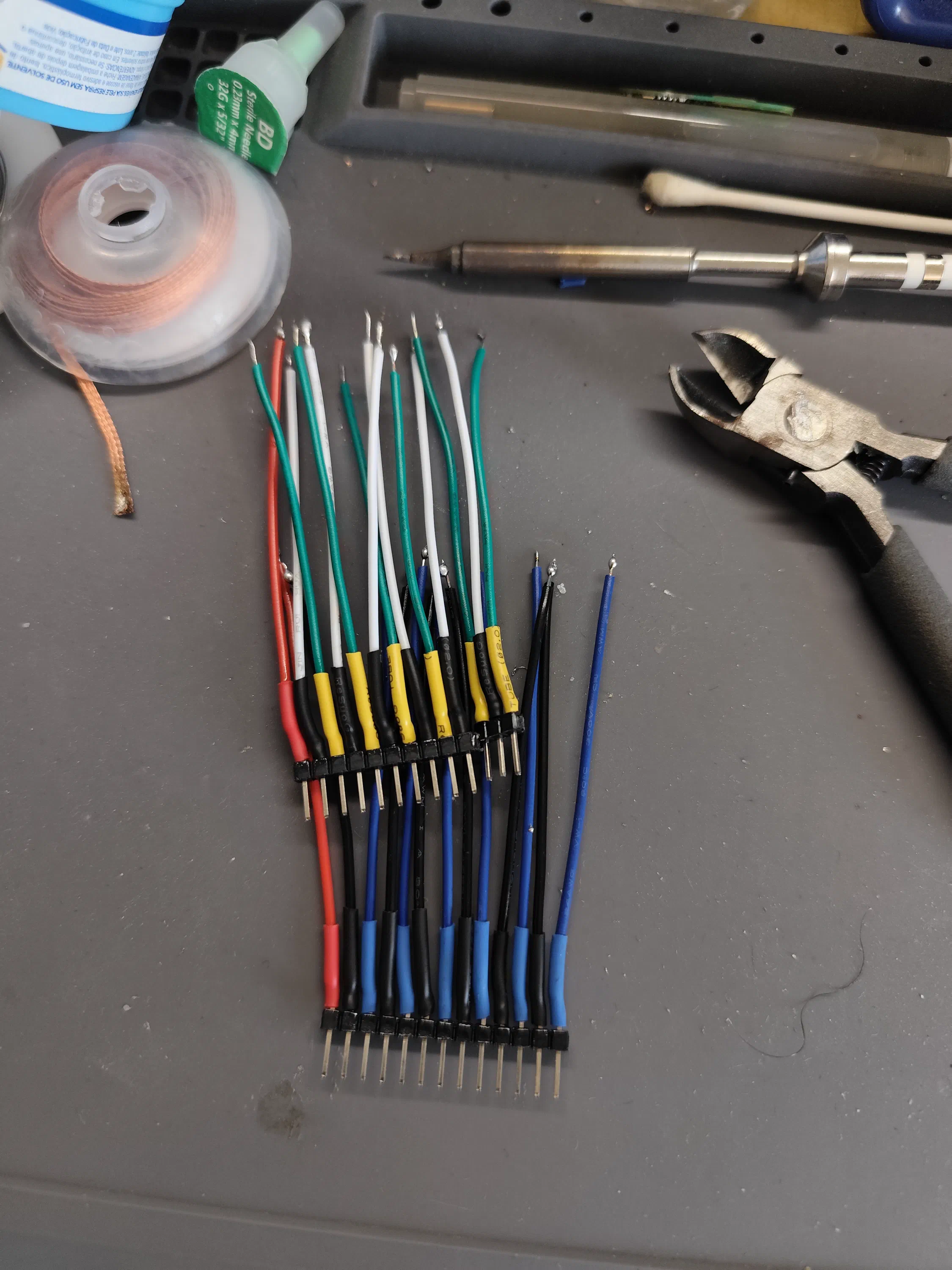
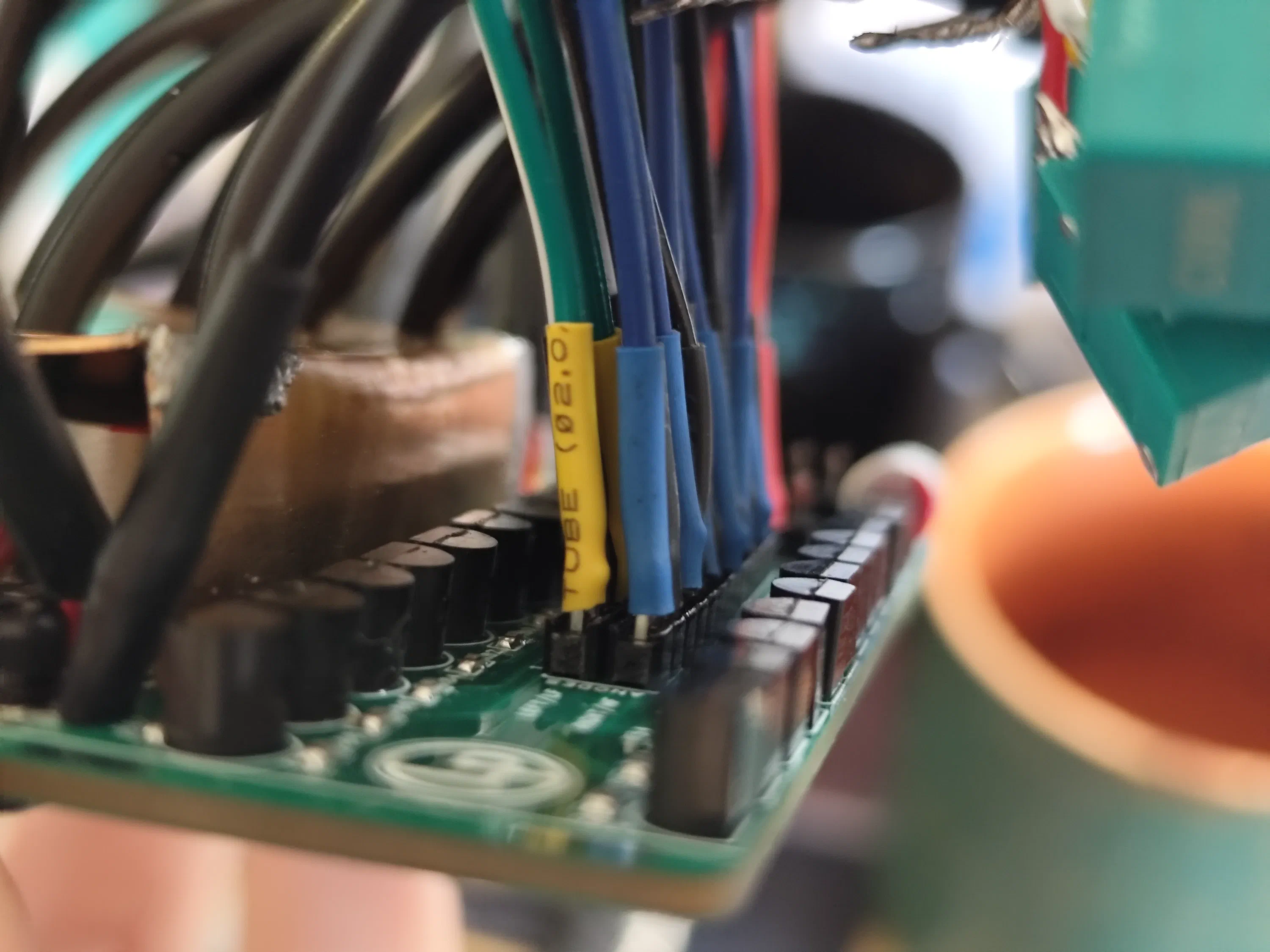
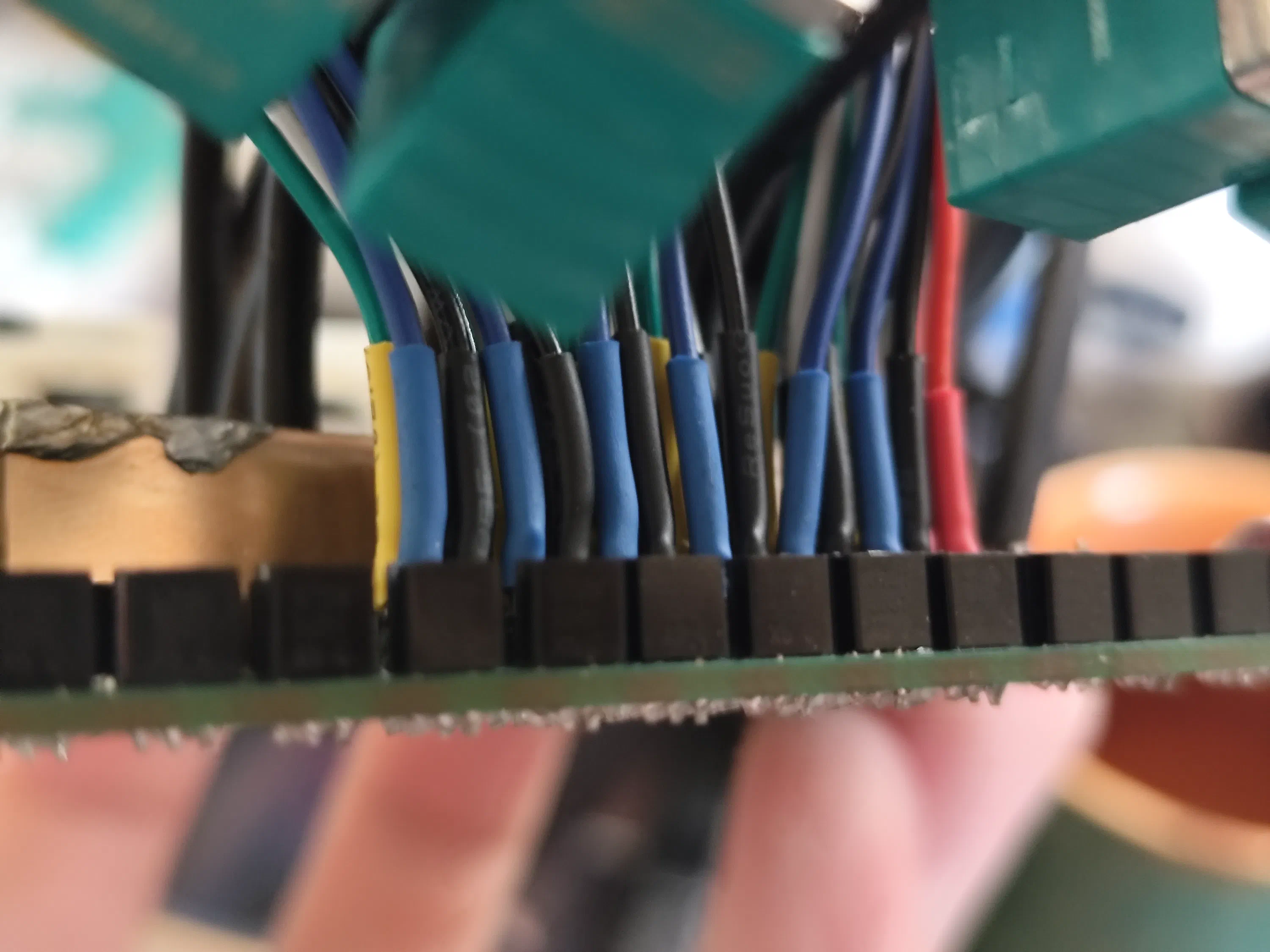
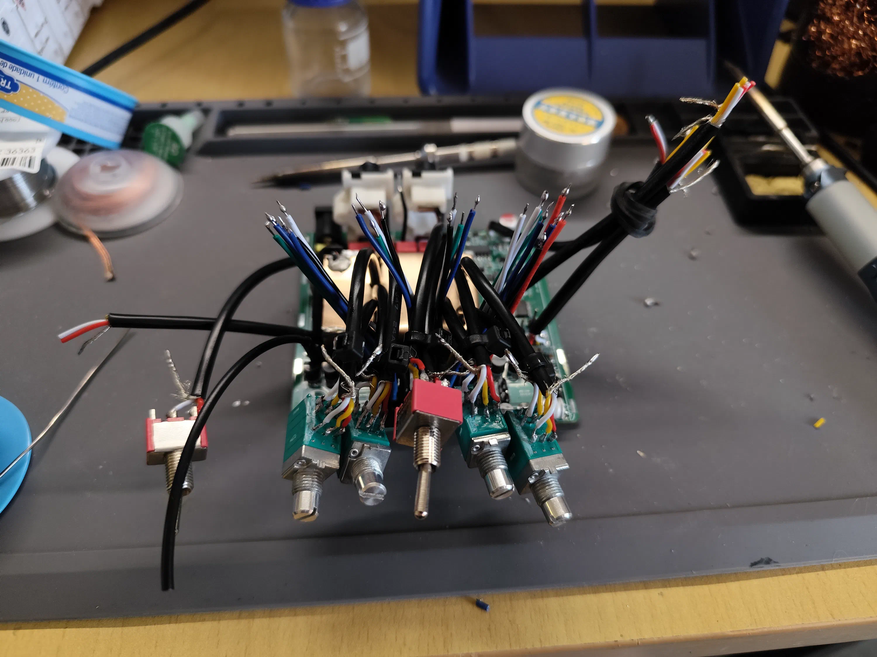
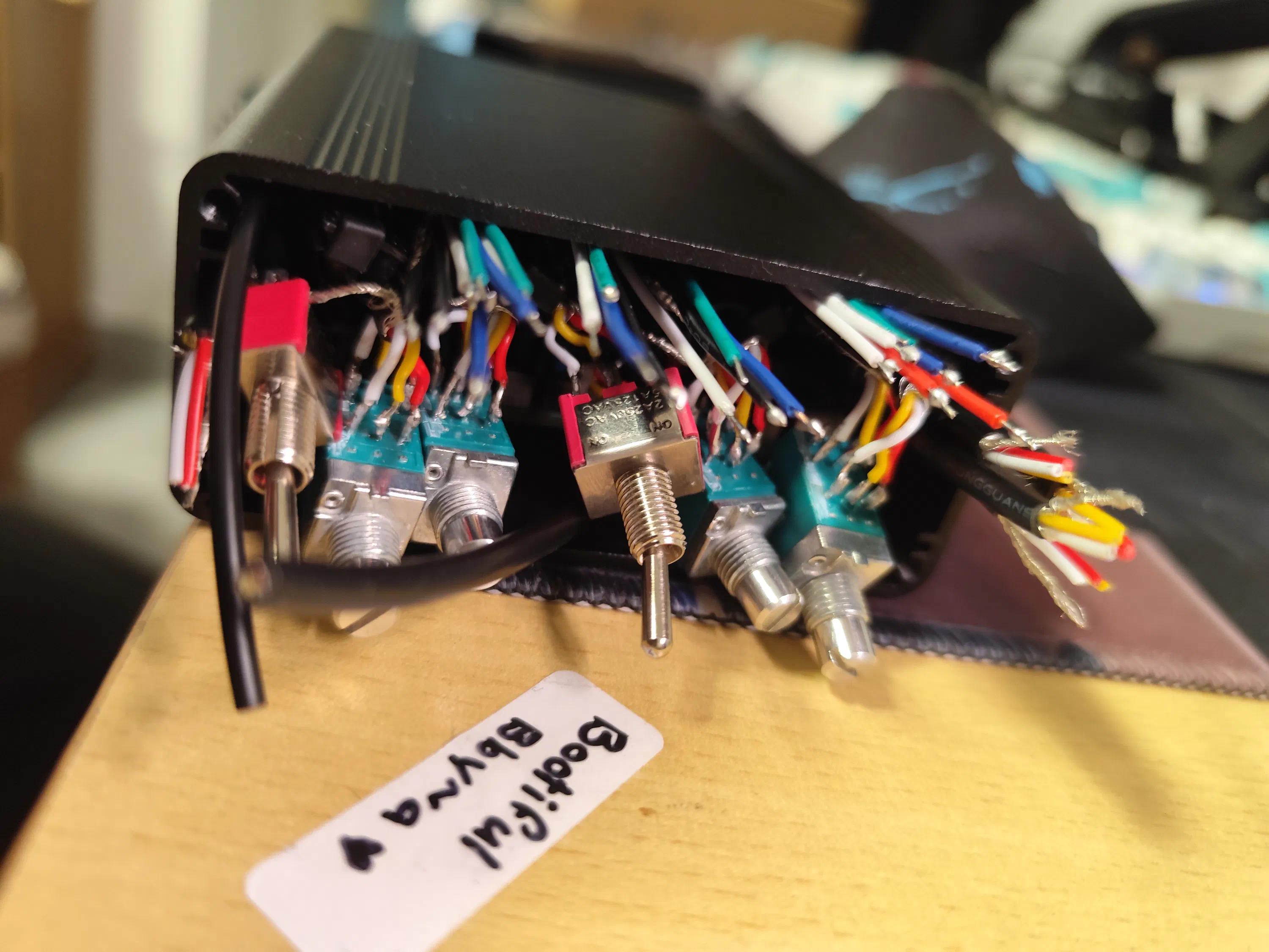
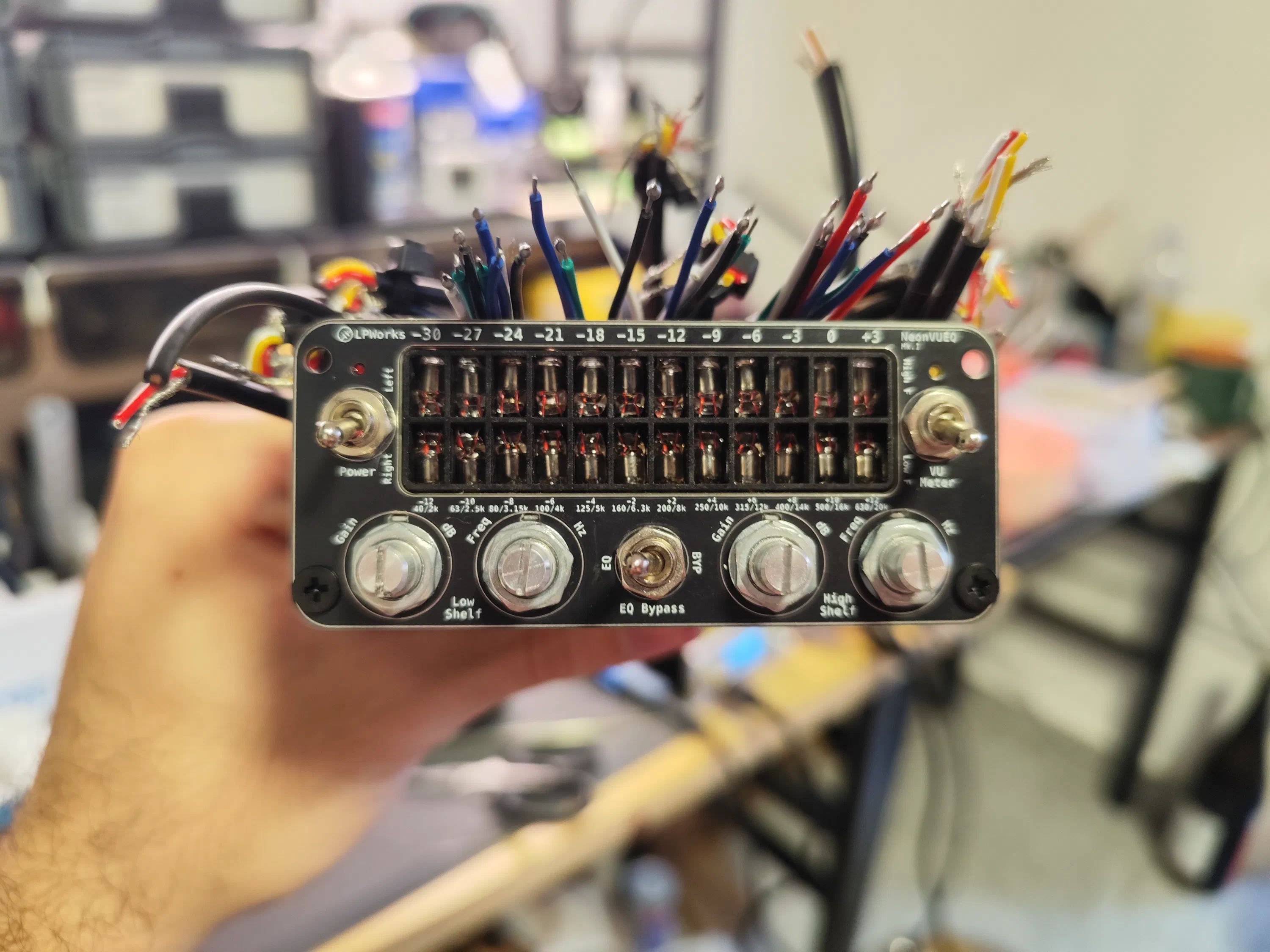
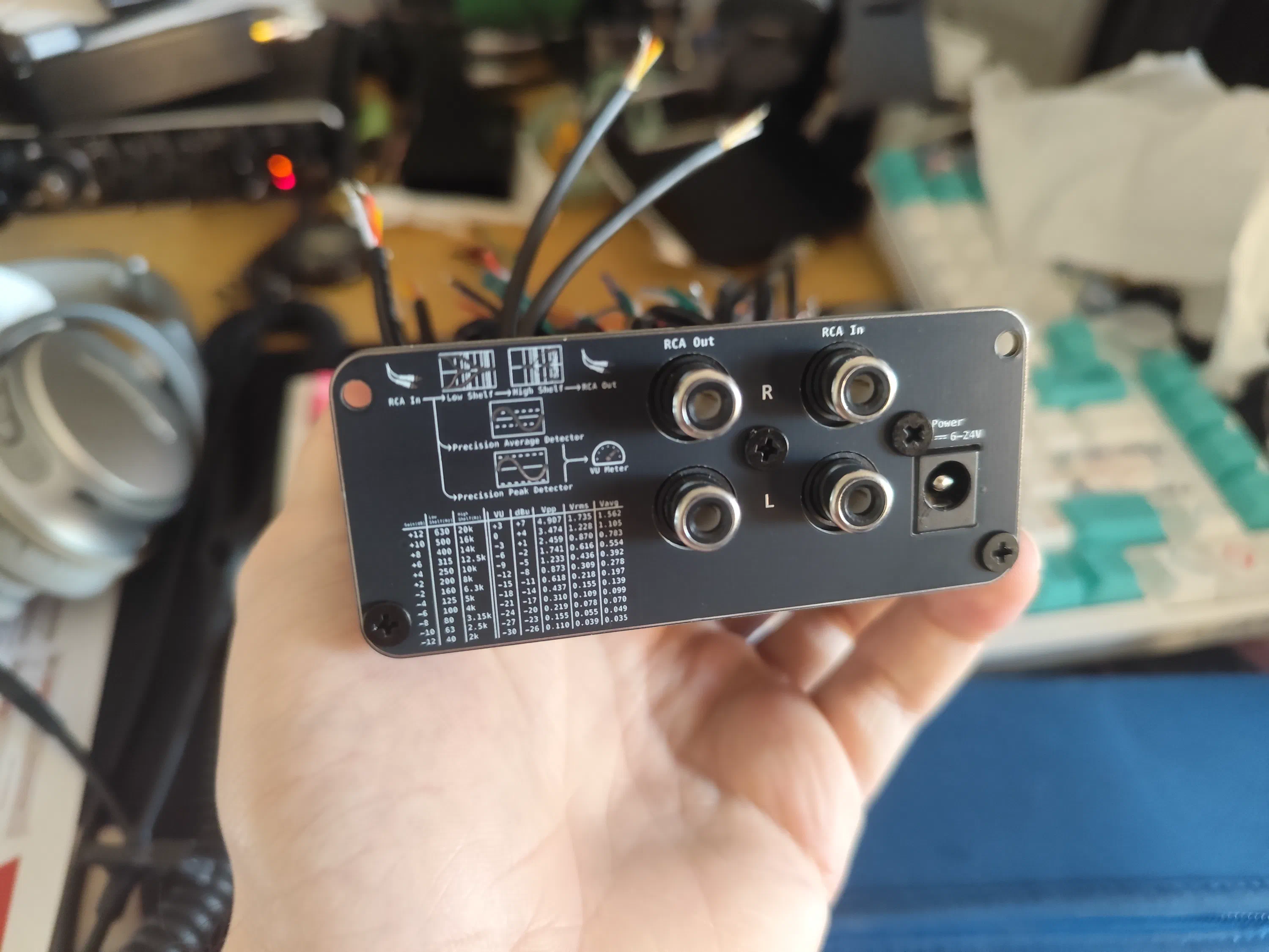
Lastly, I finished up with assembling the rear panel and mounting everything within the extruded aluminium case.
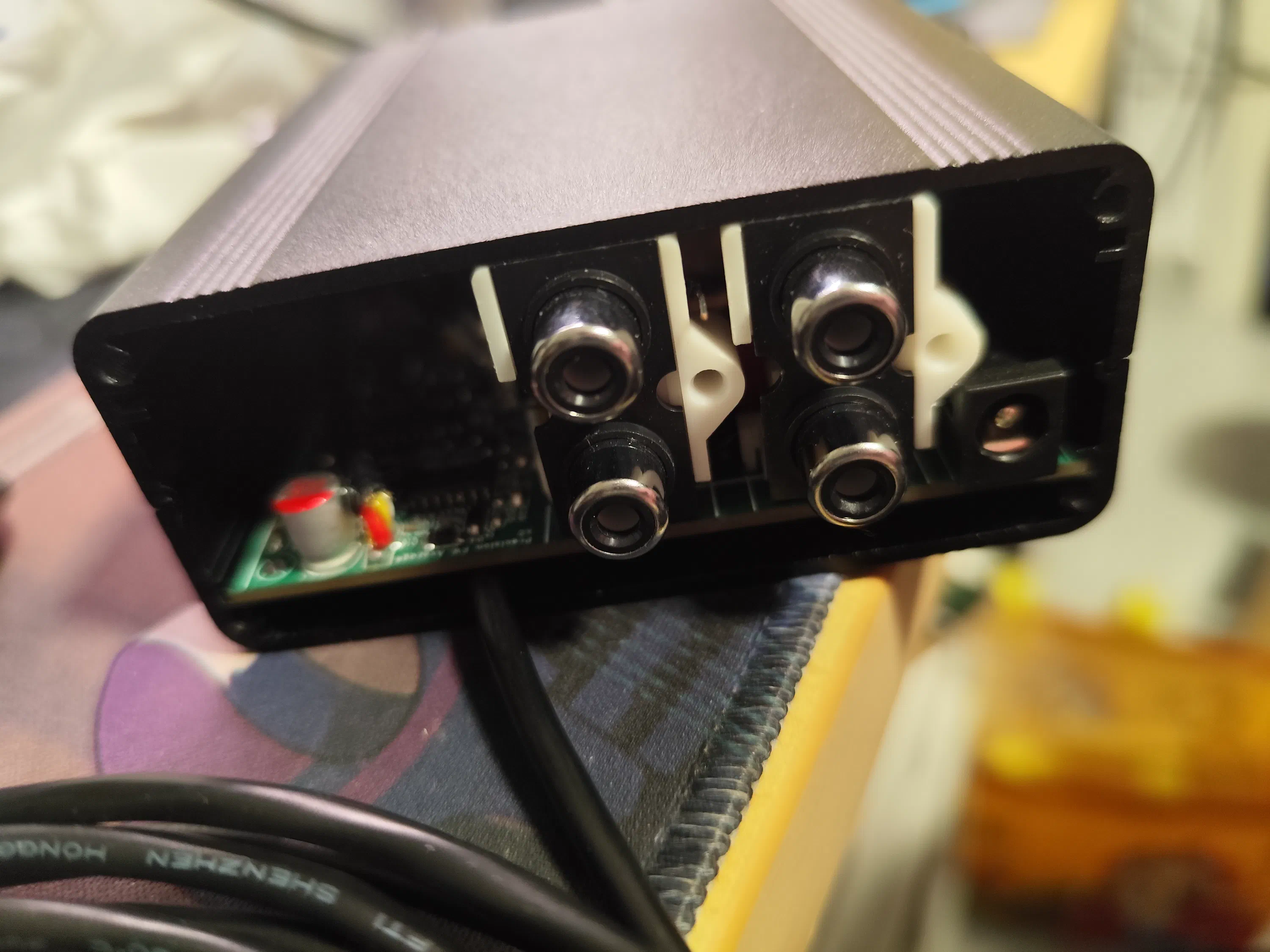
Showcase
With that, the whole project was complete.
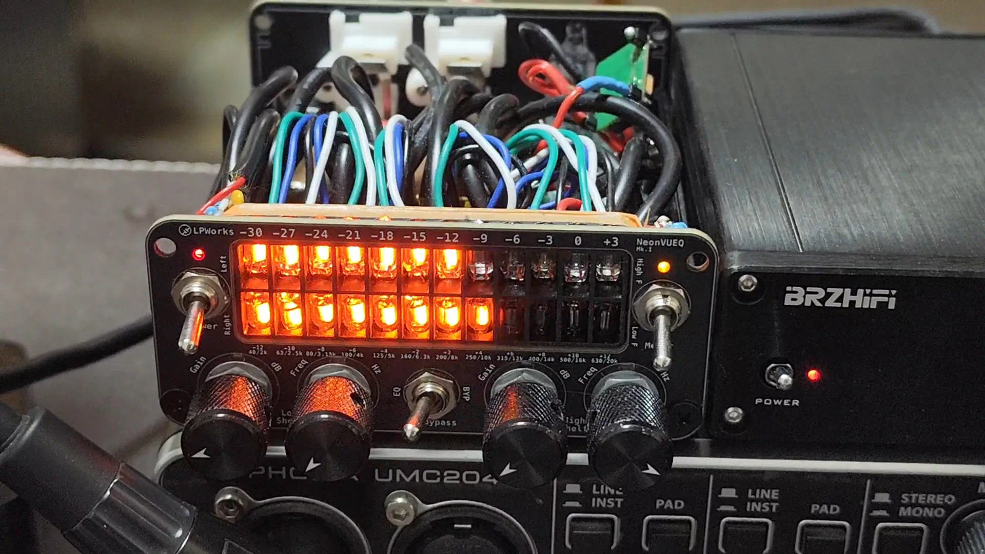
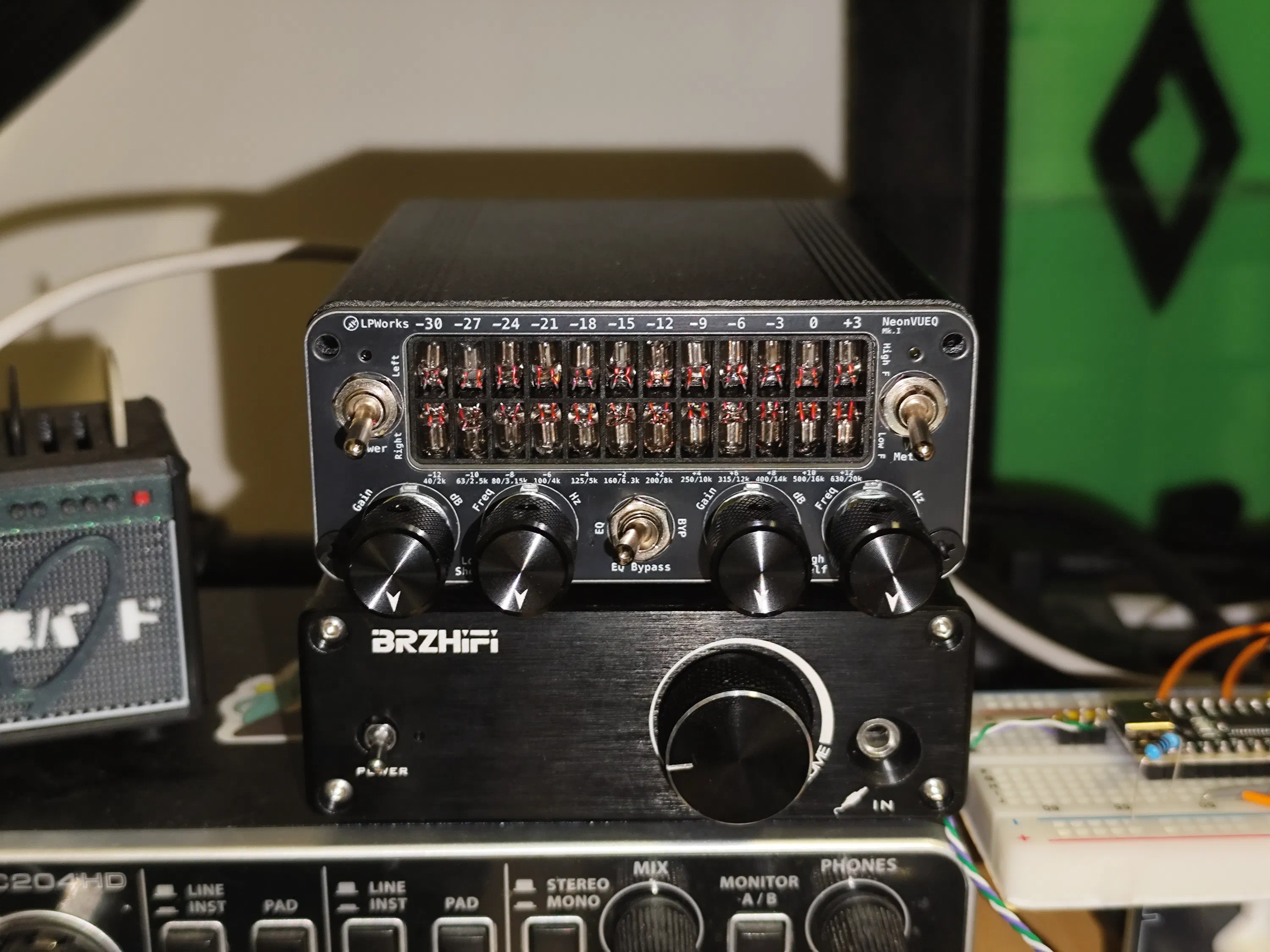
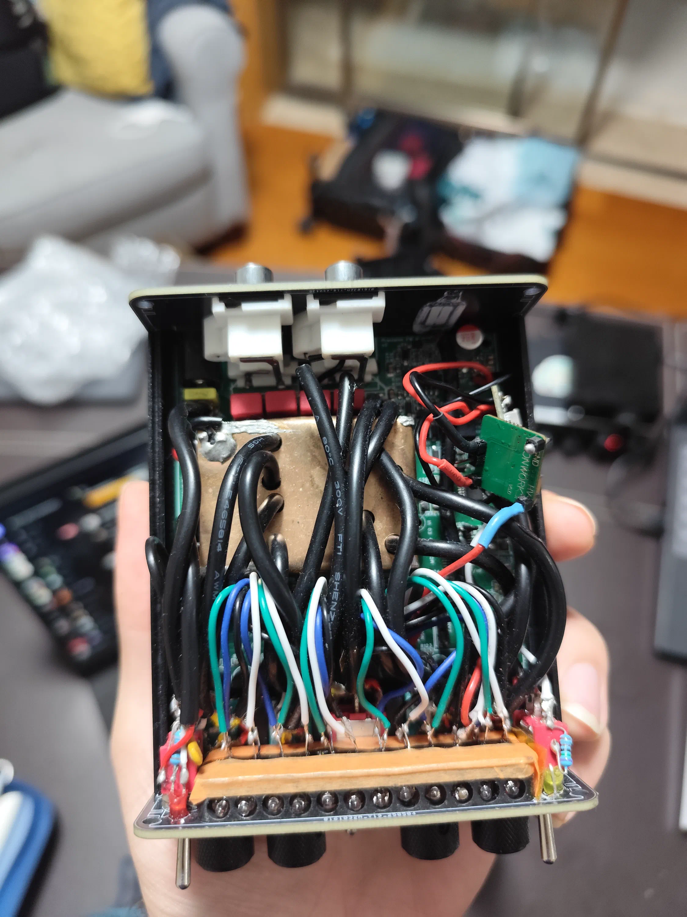
And finally, some demo videos of it in action:
Update:
As of January 2026, unfortunately one of the driver BJTs for the neons failed in short-circuit mode which destroyed the high-voltage supply and one of the MCUs with a great release of magic smoke.
This adds to the need for a future revision of this project to address that, the easy of assembly issue (much better idea to use ribbon cables rather than manually soldering everting), and actual implementation of the UI as originally intended.
Luckily the analog parts of the circuit were unaffected, and therefore I can continue using it as just an EQ for my speakers without the neon VU meter.