
UMP MkII - Part1
Contents
This is a long and painful project with many revisions, I call this the Mark II version; though honestly, this is more like the Mark IV version. This personal Digital Audio Player (DAP) project was first attempted in 2021; as a de-facto replacement to my 2016 iPod Nano 7 and it’s limited 16GB storage plus iTunes synchronisation headache. The original used a NanoPi NEO Air as it’s brains for Linux goodies. But after a tragic reversed insertion and killing of the main board on the prototype; this next revision is the first fully embedded version, switching to a STM32H7 for the brains and going all out with the embedded programming instead of using ready-made Linux solutions such as MPD.
Motivation
Why build a custom DAP in 2026?
After many years of owning various digital audio players, from nuggets in the early days, to digital Sony Walkmans, to eventually my iPod Nano 7; there has always been 3 main frustrations I’ve had with every commercial device:
- Limited storage capacity which isn’t sufficient for large music libraries (Got to say the original iPod nailed it in this regard with their mini spinning hard-drives, yet somehow by the time we get to the iPod Nano 7, 16GB was considered acceptable).
- Proprietary formats and software to sync and manage music libraries, which often lock users into specific ecosystems and leave them with zero support years later when the device or application is inevitably discontinued. This is compounded by the fact that not only do many devices not support a plain standard format library like MP3 or FLAC, but also the library management is severely lacking when it comes to organising, labelling, and tagging music for effective browsing in a large collection.
- Limited battery life, often with form factors that prioritize slimness over capacity. The whole point of a dedicated player is immediate and always ready-to-go convenience. A device that constantly needs charging defeats the purpose of having a dedicated music player over a smartphone.
While points 1 and 3 have improved a lot with modern options from HiFi audio brands, point 2 remains the biggest frustration for me. I’m yet to see some intentionally designed music library management software that truly manages to maintain and organise a large traditional file-based music library effectively. This is one of the main motivations behind building my own custom DAP. The process of adding new songs and having them labelled and synced to the device should be as seamless as possible. The iPod Nano 7 held good ground while iTunes was readily accessible, but once I no longer owned a Mac machine and iTunes was retired; I was quickly stuck with just the same old song selection and no easy way to manage, and more importantly organise, a growing music collection.
These frustrations will heavily guide the design choices for this custom DAP, with a particular focus on the library management software, on-device browsing capabilities, and ensuring a polished overall user experience with long battery life and expandable storage options.
This is my journey to create my own Ultimate Media Player; hence the name UMP.
In this first part, I’ll cover the first hardware revision of the Mark II revision based on the STM32H7 MCU. With an initial iPod-like design that set the base for the form factor and user interface. I’ll mostly cover the hardware design, UX considerations and component choices. With the software side being covered in [Part 2](todo://ENTER PART 2 LINK HERE).
Initial Design Considerations
With the key pain-points identified above, and my prior mishap with using a Linux-based SoC in the original UMP Mk1, I decided to take a different approach for the Mark II. Going all in on the software development side by opting for a more traditional microcontroller-based solution. Though an order of magnitude more development and optimisation work is needed; this approach allows me to achieve much tighter power management, better battery life, and to have full control over the hardware-software integration for an optimal user experience.
Of course this means, basically implementing my own operating system and software stack; from low-level device drivers, to audio processing pipelines with multiple format decoders, to multi-threaded task management with carefully set real-time task priorities built on top of FreeRTOS, to ensure smooth and responsive performance across all aspects of the device, from audio playback to user interface interactions. It’s a huge optimisation surface that requires careful planning and execution to get right, particularly meeting performance, memory and real-time constraints working within an MCU.
All-embedded decision aside, the other key design consideration was the form factor and user interface of the device. I find that with an ever-growing music library, UX flows for browsing it need to be intuitive and efficient. The user should be able to find the exact song they desire from thousands of tracks with minimal effort; ideally, with their eyes closed. Practically, this translates to the following requirements:
- All controls must be tactile and provide clear feedback, allowing the user to operate the device without needing to constantly look at it.
- The interface must support fast and efficient navigation without requiring many clicks or deep menu-diving operations.
Besides that, I want to make sure the device remains aesthetically pleasing, with a design that feels premium and well-crafted. After all, not only will this device be used daily for extended periods, but why settle for something that doesn’t bring joy to use and behold after already spending the significant extra effort to create an all-embedded solution?
Hardware Design
As usual, the hardware design starts by staring at a blank schematic sheet on a new EDA project. In this section I’ll elaborate on the key requirements that drove the component selection and overall hardware architecture for the Mark II design.
Component Selection
In this section I’ll breakdown which considerations went into the choice of each major component for this preliminary design.
Microcontroller
The first critical decision was selecting which microcontroller to use. While I haven’t used the STM32 series extensively before, with the ESP32S3 probably being the most performant MCU I have experience with, I was already impressed by the RP2040’s ARM Cortex-M0+ cores and the STM32H7 series promises significantly higher performance. Along with a rich set of peripherals which can be easily configured through STMCubeMX (especially I2S), this made the STM32H7 a very attractive choice for the Mark II design.
Despite being a single-core MCU, unlike the dual-core ESP32S3 and RP2040’s I’ve used in the past; the ARM Cortex-M7 core in the STM32H7 offers a really high single-core performance, included double-precision floating-point unit (FPU) (critical for real-time DSP audio processing), and full FreeRTOS support. This makes it quite the beast for handling demanding audio processing tasks while multitasking efficiently. It’s advanced memory architecture, including an MPU and tightly-coupled memory regions, data and instruction cache, and absurd core clock speed up to 480 MHz make it incomparable to any class of MCU I have used before. Feeling more like an SoC class part than a traditional microcontroller, while still having excellent software support, and the handy SWD ARM debugging interface which made development and debugging significantly easier compared to my previous experiences with other MCUs.
Prototype Dev Board
To validate the feasibility and get a feel for the power packed in the STM32H7, I started with a STM32H743 development board and a simple PCM5102A DAC for audio output. This allowed me to quickly prototype and test the audio processing capabilities of the MCU, ensuring that it could handle the demanding real-time DSP tasks required for the Mark II design; supporting multiple complex decoders for FLAC, MP3, and OPUS, while still having enough headroom for a DSP pipeline and UI rendering.
While the software will be covered in a later part, this initial dev board test positively surprised me, as the STM32H7 was able to handle every demanding task I threw at it with ease. Making it a solid foundation for the Mark II design and giving me confidence that the MCU could meet the performance requirements for both audio processing and user interface tasks.
Microcontroller Peripherals
One difficult choice to make when designing with the STM32H7 family is deciding how few add-on peripherals you can get away with while meeting the requirements for your project. While the STM32H7 comes with a rich set of built-in peripherals, it is also common and often necessary to add external flash memory for additional program or data storage, as well as external RAM for buffering and other large data processing operations. These external peripherals can quickly inflate the total pin count needed and force the use of a larger package MCU or more complex PCB routing to accommodate all the necessary connections. Increasing both device size and cost.
It became pretty clear early on that additional external flash was going to be needed, in the least to store CJK fonts that will be used for the user interface to support Chinese, Japanese, and Korean characters. Beyond that, the firmware itself is rather large due to the many complex algorithms for audio decoding and DSP. A simple W25Q64 over SPI suffices for these needs. However, a tighter requirement was the amount of available built-in RAM, as external SDRAM is huge and requires many carefully length-matched traces; something I wanted to avoid if at all possible. I bit the bullet with this one, and decided to crunch on code optimisation and memory management to make the most out of the 1MB internal RAM.
A more nuanced decision was the limited speed of the built-in USB FS PHY, which only supports 12Mbps (1.5MB/s theoretical max USB speed); which is a huge bottleneck for music library synchronisation using USB Mass Storage Class (MSC) mode. To overcome this limitation with the STM32H743 specifically, there is no choice but to use an external USB HS (480Mbps) PHY connected over the ULPI interface, which adds complexity to the design but is necessary to achieve the desired USB performance. I later came to regret this, as it significantly increased the design complexity and required careful signal integrity considerations, making the PCB layout more challenging than initially anticipated. A better solution trade-off is made in [Part 3](todo:// add part 3 link here).
Audio DAC
When it comes to the audio DAC selection, this was quite easy, as I had no doubt in my mind. I opted for the CS43131 from Cirrus Logic, as it is my daily driver DAC that I use with my iBasso Macaron dongle; and it offers outstanding audio quality, low power consumption, and a compact footprint, making it an ideal choice for the Mark II design.
While it does introduce some additional complications, such as needing a 1.8V level shifter for all the I2S lines, can careful PCB layout for it’s integrated charge pump and careful power supply design to achieve it’s noise specifications. The effort is well worth it for the audio quality it delivers, and I would not settle for anything less. It is one of the de-factor choices for high-quality portable audio DACs, and the most critical component for achieving high audio performance and fidelity for a portable DAP.
Storage
For storage, a relatively cheap and large capacity solution is needed. While at first I really wanted to use eMMC NAND flash for its reliability and relatively low cost per GB, it has a major problem; the required BGA-153 footprint is quite high density and would require PCB manufacturing specifications beyond what is commonly available in standard tiers. Greatly increasing the price and complexity of manufacturing the device.
For that reason, there was really only one option left, which was to use SD card storage. SD cards offer a good balance between cost, capacity, and ease of integration; but I have a personal vendetta against microSD cards due to their extreme fragility and tendency to get lost or damaged easily. Therefore, I opted for full-sized SD card slots, which provide a more robust and reliable storage solution, at the cost of increased physical space on the PCB and the enclosure. I later came to regret this decision when doing the PCB routing.
Power Management
Power management has always been a tricky aspect of my projects, as it can easily ruin a project if not properly designed. Another key feature that I absolutely needed besides efficient idle power consumption, was robust battery monitoring capability to report an accurate battery level gauge. This is an area where there are many complex trade-offs in the choice of power management ICs; with many pitfalls with complex solutions, and frankly, not many options to choose from. After careful research and consideration, I settled on a three part power solution; consisting of separate step-up converter, battery charger and fuel gauge ICs.
The step-up converter is the most critical part in the PSU system, as it’s idle current consumption characteristics can make-or-break the overall power efficiency goals of the device. Therefore, I carefully selected a step-up converter with ultra-low quiescent current and high efficiency across a wide load range, ensuring minimal power loss during both active and idle states; especially as I plan to have no physical power switches and rely entirely on the device’s power management circuitry for controlling power states. I settled on the TPS61023 from Texas Instruments, as it can provide the main VSYS 3.3V rail effectively with pass-through mode when the LiPo battery voltage is higher than 3.3V; while boasting an ultra-low 20uA quiescent current in auto PFM operation at light load.
The battery charger chosen was the Texas Instruments BQ25185. It has a simple GPIO interface, and most importantly an integrated power mux. Allowing us to seamlessly switch in USB power when available to VSYS for the battery charger IC, without external components or interruptions.
Last, a simple but hopefully effective fuel gauge IC was choosen; the LC709203, from Onsemi. This IC provides a I2C interface for monitoring the state and unlike traditional Coulomb counter-based fuel gauge designs, it simply uses a direct battery voltage measurement with a well-calibrated internal lookup table algorithm to estimate the remaining battery capacity accurately. This approach simplifies the design and reduces potential sources of error, while still providing reliable battery level information for the system.
User Interface
The user interface provides some creative challenges for this project, as it needs to be both intuitive and tactile while also fitting within the form factor constraints and incorporating a method for fast user input for scrolling through large lists of content efficiently.
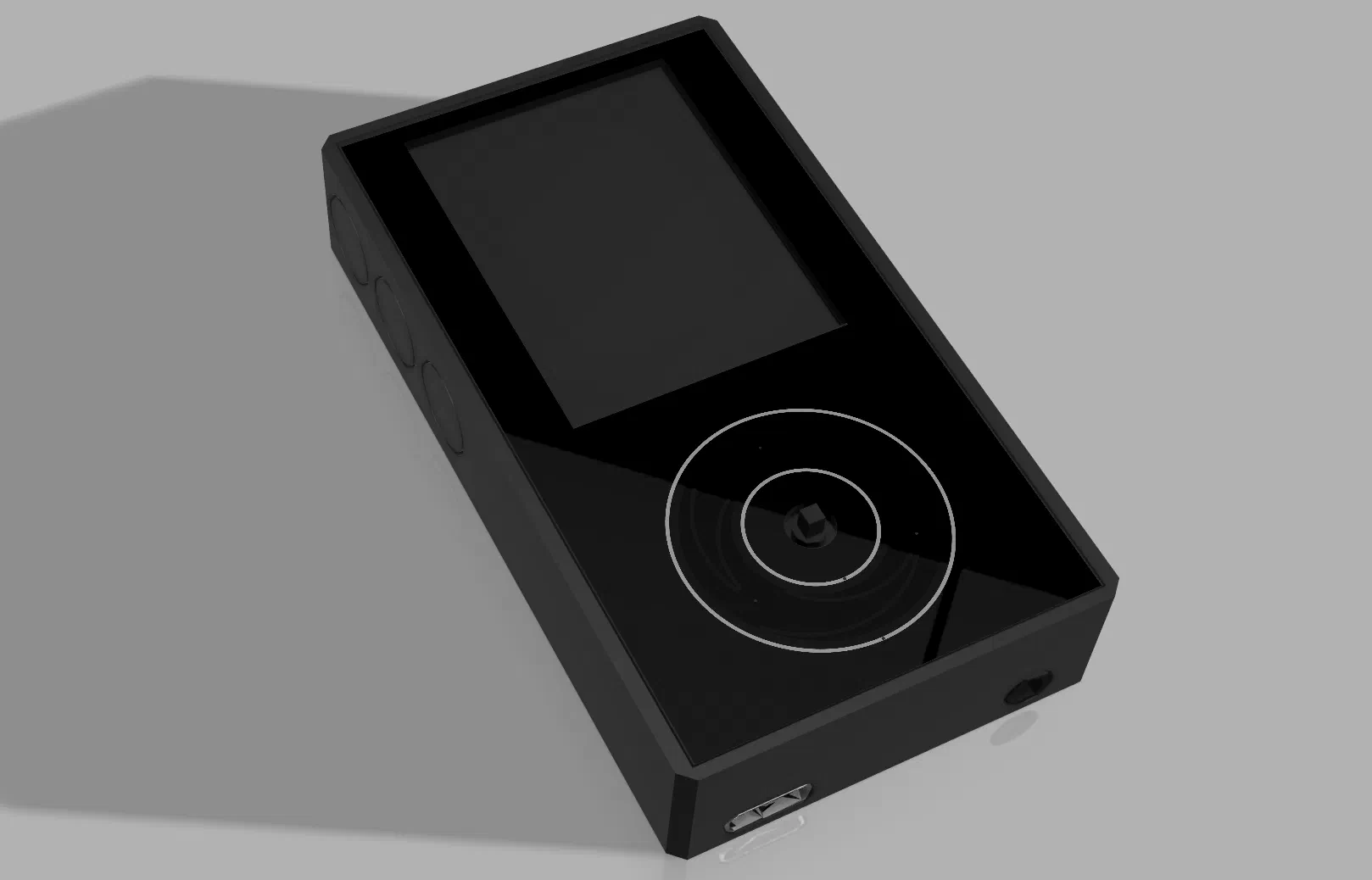
To solve these requirements, I decided to take some inspiration from the original iPod click wheel interface, which allows for fast and intuitive navigation through large lists of content with minimal physical controls. Implementing a similar tactile touch-sensitive wheel plus button interface on the other hand, posed it’s own set of challenges. I employed an Atmel AT42QT2120 capacitive touch controller for the wheel, which features a native capacitively interpolated slider position sensing capability; allowing us to simple read position values from 0-255 interpolated between 3 repeating and overlapping touch electrodes along the wheel. This greatly simplifies the firmware implementation for detecting wheel rotation and direction, as the touch controller does the heavy lifting of interpreting raw touch signals into meaningful position data. This was paired with a 5-way mechanical switch in the center for discrete button inputs, providing a familiar and responsive user interface for menu navigation and selection actions. Combined these form a neat package that balances tactile feedback with intuitive touch-based navigation, but it wouldn’t be complete without tactile feedback for the wheel itself. Which is achieved by using a small Linear Resonant Actuator (LRA) motor with a DRV2605 driver IC to provide true haptic feedback. This driver IC has a built-in library of vibration effects and should greatly elevate the user experience. With haptics being somewhat of an expected commodity on modern smartphones, it really is something that once you have felt, you cannot go back to not having.
Besides this main input package, the rest of the UI is a fairly standard combination of a small 320x240 TFT display, and a 3 button transport/volume control strip.
PCB Layout
With all the major components decided, I started with the PCB layout by carefully planning the STM32H743 and peripheral’s placement. Of course I aimed for the smallest viable footprint, targetting a device around the size of my original iPod Nano 7, though much thicker for the additional battery capacity requirements.
We start with the layout of the connectors as usual, with the USB-C and the audio jack placed along the bottom, and the full-size SD card slot along the top edge for easy access. This leaves us with just enough space to place the navigation buttons on the left and the screen and front-panel ribbon cable connector on the right and bottom, with the STM32H743 in the center.
The stack-up is a 4 layer board with a Signal-Ground-Signal-Ground topology; as there are no bottom layer components.
Mechanical Design
In order to cut costs while still providing a premium enclosure experience, I went with a PCB sandwich layout; with the main board as the bottom case panel, a SLA 3D printed or aluminium CNC machined outer frame, and a top PCB front panel. This approach allows for a sturdy and visually appealing enclosure while keeping manufacturing complexity and costs relatively low.
Enclosure Design
The enclosure design follows the PCB sandwich concept, with careful attention to the placement of cutouts for the display, buttons, and connectors. The outer frame provides structural integrity, while the top PCB front panel ensures a clean and professional appearance; including silkscreen print labels and silver copper highlights for added visual appeal. This modular approach also allows for easier assembly and potential future upgrades or modifications.